 Photonic Materials Technology Section (PMTS)
Nano-Electronic Materials and Devices Laboratory
Photonic Materials Technology Section (PMTS)
Nano-Electronic Materials and Devices Laboratory
Visible and Solar Blind UV Photodetectors
Visible blind UV photodetectors are important for multiple applications such as missile plume detection, arc flash, flame and combustion monitoring, environmental monitoring, and industrial quality control, UV communication etc. We have developed UV photodetectors based on wide bandgap semiconductors MgZnO and Ga2O3 thin films with following details.
MgxZn1-xO based visible blind M-S-M UV Photodetectors
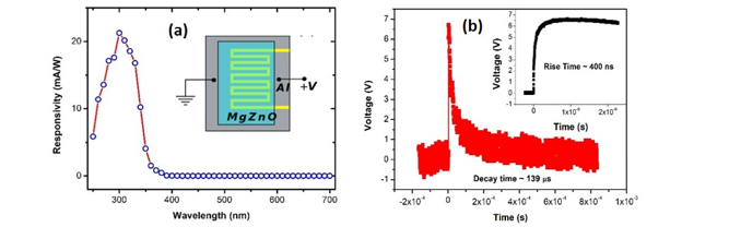
We have in-house developed photoconducting type visible blind UV photodetectors using MgxZn1-xO thin film in planar metal-semiconductor-metal (MSM) geometry. The Mg0.15Zn0.85O thin film (bandgap ~ 3.6 eV) of thickness ~ 100 nm was deposited by pulsed laser deposition over sputter deposited Al interdigitated metal electrodes on glass substrates, followed by in-situ deposition of ~ 90 nm thick MgO capping layer to improve the device stability. The typical spectral responsivity and temporal response of Mg0.15Zn0.85O based MSM photodetectors are shown in Fig. 1.
|
Fig. 1. (a) spectral responsivity and (b) temporal photoresponse following a 20 ns laser pulse at 248 nm of the Mg0.15Zn0.85O MSM UV photodetector at 20 V bias. The device schematic is shown in in inset. |
The optimized Mg
0.15Zn
0.85O MSM UV photodetectors showed following characteristics:
- UV to visible rejection ratio ~ 2.7×10⁴
- Responsivity ~ 20 mA/W at 310 nm (20 V bias)
- ON/OFF ratio ≥ 102
- Cut-off wavelength ~ 350 nm
- Photocurrent rise and fall time ~ 400 ns and 139 µs (measured using 20 ns laser pulse)
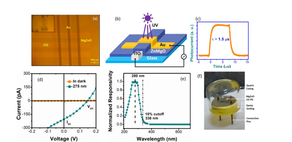
Self-powered visible blind UV photodetectors based on MgxZn1-xO vertical Schottky junctions
In order to achieve ultrafast response in MgZnO based self-powered Schottky type visible blind UV photodetectors, it is crucial to decrease both the junction capacitance and carrier transit time. To meet these criteria, Au/MgZnO/ITO Schottky junction photodetectors have been realized in 3×3 crossbar pattern, wherein the thickness of the MgZnO thin film deposited on patterned ITO-glass substrate is ~ 200 nm and the lateral device dimension is 320 µm×100 µm with cross-sectional area of the devices ~0.032 mm2. The semi-transparent ~10 nm Au electrode on top of the MgZnO film served as the Schottky electrode through which light entered the devices. The vertical geometry of the cross-bar pattern and the associated small device cross-section resulted in a low junction capacitance of the devices ~ 27 pF at zero bias, which in turn produced fast visible blind self-powered ultraviolet (UV) photoresponse with following parameters:
- Cutoff wavelength ~ 320 nm
- UV to visible rejection ratio ~ 104
- Peak responsivity ~ 50 mA/W at zero bias
- Dark current: ~ 1 nA
- Response time ~ 1.5 µs (rise and fall times)
- Open circuit voltage ~ 0.3 V @ 50 µW, 295 nm illumination
|
Fig. 2: (a) The optical image, (b) schematic, (c) temporal photoresponse, (d) current-voltage curve, and (e) spectral responsivity of Au/MgZnO/ITO crossbar Schottky junction devices. (f) An indigenously packaged Schottky type MgZnO UV photodetector. |
The Au/MgZnO/ITO Schottky photodetectors in cross-bar pattern, with optimized device area, could be useful in applications requiring fast response, such as secure UV communication and UV imaging.
Ga2O3 based solar blind UV photo-detectors
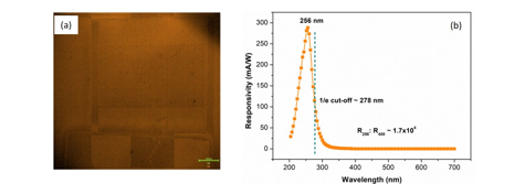
The wide bandgap semiconductor gallium oxide based solar blind UV photodetectors in M-S-M device geometry with planer inter digital ITO electrodes (digit width~40 µm, digit spacing~50 µm) fabricated in-house using photolithography showed following parameters:
- Cut-off wavelength ~ 280 nm
- Peak responsivity ~ 288 mA/W @ 5 V and ~260 nm
- UV to Visible rejection ratio ~ 104
- Dark current: ~ 290 pA @ 5 V
Fabrication and testing of Ga
2O
3 based vertical Schottky junction devices for fast and self-powered solar blind UV photo-detectors are underway
|
Figure 3: (a) Optical microscope image and (b) spectral responsivity of Ga2O3 based MSM UV photodetector. |
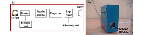
Arc flash detection system based on in-house developed UV photodetector
An arc flash caused by electrical faults or mechanical non-contact such as insulation failure, short circuit, partial disconnection, and poor contact etc., emits significant UV light, so it can be detected by optical methods. Towards this, an Arc flash detection system based on solar/visible blind UV photo-sensors has been developed which respond to UV light present in electric arc in presence of ambient light. The wide bandgap semiconductors MgZnO or Ga2O3 based UV photo-sensors with inter digital electrodes, fabricated in-house using photolithography, was connected to a trans-impedance amplifier followed by logic and alarm circuits to develop an arc flash detection system that can work in the background of visible light.
|
Fig. 4: (a) Block diagram and (b) image of Arc flash detector |