|
|
| Laser Materials Processing Division |
Development of characterization tools
Transient photo-conductivity studies |
Various transient photo-conductivity experiments such as time of flight (TOF), Photoinduced charge extraction in linearly increasing voltage (Photo-CELIV) etc. were employed to investigate charge transport in thin films for photovoltaic application. Studies on pristine and doped thin films of Poly(2-methoxy-5-(3′,7′-dimethyloctyloxy)-1,4-phenylenevinylene) (MDMO PPV) showed the role of casting solvent and nano-material dopants in governing the polymer film morphology and charge transport.
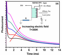 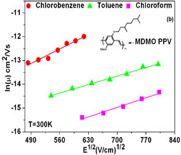
(a) Typical variation of TOF pulses with applied electric field (b) Field dependence of mobility in MDMO PPV thin films casted using different solvents. Inset shows principle of TOF.
|
| |
Steady state photoconductivity studies |
Photo action spectra (PAS) of MDMO PPV thin films under forward upon illuminating through cathode and anode was investigated to understand the role of photoinjection at electrodes. Under forward bias, PAS upon illumination through cathode and anode looked similar to photoluminescence excitation (PLE) spectra, which suggested that the carrier generation is truly a bulk process and photoinjection of holes near anode is inefficient.
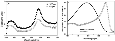
PAS of MDMO PPV thin films under forward bias (b) absorption and PLE spectra of MDMO PPV thin film |
| |
Flash-Photolysis Time Resolved Microwave Conductivity Experimental Setup |
Flash-photolysis time-resolved microwave conductivity (fp-TRMC) is a pump-probe based highly sensitive and contact less technique for studying the complex photoconductivity in variety of nanomaterials which are in the form of solution, solid or gas-phase. TRMC will be used to determine the total mobility and lifetime of induced charge carriers and to distinguish between direct and trap-mediated recombination mechanisms in photoactive materials useful for photovoltaic and photocatalytic applications. Development of TRMS set up is being carried out and we have characterized various sub components of the system such as Gunn Diode, Isolator, Circulator and detector etc. Design and fabrication of microwave resonant cavity is under progress. |
| |
Monte Carlo simulation studies on charge transport |
Influence of polymer film morphology on charge transport in semicrystalline conjugated polymer films were investigated using Monte Carlo simulation. A model with simulation codes was developed to delineate charge transport in semicrystalline polymer thin films. Simulation results provided the variation in charge transport parameters upon changing the film morphology. Further investigations provided deeper insight on how the field and temperature dependence of mobility, carrier diffusion, photocurrent pulses etc are intricately connected to the polymer film morphology. |
Soft X ray excited optical luminescence (XEOL) setup for characterization of luminescent materials |
Soft X-ray excited optical luminescence (XEOL) is a process in which X rays excite the sample and fluorescence in visible and near visible is measured. With the tuneable X ray sources like Synchrotron radiation source (Indus 1), the absorption edge can be tuned close to elements specific absorption edge. Due to short absorption length (~100-1000 nm), surface specific optical properties of light emitting and photovoltaic nanomaterials can be studied. We therefore developing a XEOL set up at the reflectivity beamline (BL-4 of Indus 1). A dual lens based probe for collection of fluorescence from the sample to the fiber coupled with the spectrograph developed. For initial studies we recorded photoluminescence from cerium doped yttrium aluminium garnet (Ce:YAG), a well known scintillator material for detection of ionizing radiation, as a standard sample for the demonstration of the setup.
Facilities developed:
- Wet chemistry lab equipped with fume hood, vacuum oven, hot plate and spin coater, ultrasonic bath cleaner etc.
- Integrated glove box system with thermal evaporation system for device fabrication in inert environment
- Steady state and time resolved photoluminescence measurement (UV-VIS-NIR) system (decay time from ~200 ps to microsecs, RT temp to 10K and emission range 300nm to 1600nm)
- Transient and steady state photoconductivity measurement system
- Polymer poling setup for developing NLO materials
- Surface profiler for thickness and roughness measurement
- Wavelength tuneable Nd:YAG based pulsed OPO laser (tuneable range ~ 410-1800nm)
- Temperature controlled electro-deposition setup
- Thermal evaporation system
- Thin film impedance measurement system
- Optical absorption spectrometer
- Contact angle measurement system
- Solar simulator
- Plasma cleaner system for surface cleaning
- Stereo zoom microscope for micro devices inspection
- Source measurement unit for I-V and C-V characterisation of devices
- Liquid and vacuum phase pulse laser deposition setup with YAG laser as source.
Facilities under development
- Femtosecond laser based micro/nano structure fabrication facility
- Thermally stimulated current/photoluminescence measurement setup
- Soft X ray excited optical luminescence (XEOL) measurement setup at BL-4 on INDUS 1
- Time resolved microwave conductivity measurement system
|
| |
Related publication since last five years |
- Chethan Pai S, M. P. Joshi, S Raj Mohan, T. S. Dhami, Jayakrishna Khatei, K S Koteshwar Rao , L. M. Kukreja and Ganesh Sanjeev, “Effect of electron beam irradiation on photoluminescence properties of thioglycolic acid (TGA) capped CdTe nanoparticles”, Adv. Mater. Lett 4(6), 454-457(2013).
- Kolli, B., Mishra, S.P., Joshi, M.P., Raj Mohan, S., Dhami, T.S., Samui, A.B. “Click chemistry-based synthesis of azo polymers for second-order nonlinear optics” J. Polym. Sc., Part A: Polymer Chemistry 50 (8) , 1572-1578 (2012).
- Balakrishna Kolli, Sarada P. Mishra, M. P. Joshi, S. Raj Mohan, T. S. Dhami, L. M. Kukreja, A. B. Samui, "Synthesis and Characterization of Y-type Polymers for Second Order Nonlinear Optical Applications" J. Poly. Sci. A: Poly. Chem. 51, 836(2013).
- Balakrishna Kolli , Sarada P Mishra , M. P. Joshi , S Raj Mohan , T. S. Dhami , A. B. Samui , “Synthesis and characterization of linear polymers for Non-Linear Optics through click chemistry route “, Advanced Materials Research 584, 8 (2012).
- “Effect of electron beam irradiation on photoluminescence properties of thioglycolic acid (TGA) capped CdTe nanoparticles”, Chethan Pai S, M. P. Joshi, S Raj Mohan, T. S. Dhami, Jayakrishna Khatei, K S Koteshwar Rao , L. M. Kukreja and Ganesh Sanjeev, Adv. Mater. Lett 4(6), 454-457(2013).
- “Vapor phase synthesis of hexagonal shaped single crystal yttria stabilized zirconia nanoparticles using CO2 laser”, J. Khare, H. Srivastava, C. H. P. Singh, M. P. Joshi, L. M. Kukreja,Ceramic International, 39 (2) , 1103 (2013)
- "Synthesis and Characterization of Y-type Polymers for Second Order Nonlinear Optical Applications" Balakrishna Kolli, Sarada P. Mishra, M. P. Joshi, S. Raj Mohan, T. S. Dhami, L. M. Kukreja, A. B. Samui, J. Poly. Sci. A: Poly. Chem. 51, 836(2013).
- “Electron irradiation effects on TGA-capped CdTe quantum dots”, Chethan Pai S, M. P. Joshi, S Raj Mohan, U. P. Deshpande, T. S. Dhami, Jayakrishna Khatei, K S Koteshwar Rao , and Ganesh Sanjeev,J. Phys. D: Appl. Phys. 46, 175304 (2013).
- “Synthesis and Characterization of Azo–Bisbenzylidene-Based Polymers for Second Order Nonlinear Optics”, Balakrishna Kolli,Someshwarnath Pandey,Sarada P. Mishra,Tapan Kanai, Mukesh P. Joshi,Raj S. Mohan, Tham Singh Dhami, Lalit Mohan Kukreja, Asit Baran Samui , J. Poly. Sci. A: Poly. Chem, 51, 4317–4324(2013).
- “Monte Carlo simulation of charge transport in disorderd organic thin films: Applicability of Meyer-Neldel Rule for extracting energetic disorder, S. Raj Mohan, M. P. Singh, M. P. Joshi, L. M. Kukreja, Proc. XIX International Workshop on the Physics of Semiconductor Devices AIP Conf. Proc. 1512, 940 (2013).
- “Second harmonic generation from corona-poled polymer thin films of Y-shape chromophore with different isolation groups”, Mukesh P. Joshi, Raj S. Mohan ,Balakrishna Kolli, Sarada P. Mishra, Akshaya K. Palai, Tapan Kanai, T. S. Dhami, L. M. Kukreja, A. B. Samui,Pramana-J. Phys., 82, 283 (2014).
- “On red – shift of UV photoluminescence with decreasing size of silicon nanoparticles embedded in SiO2 matrix grown by pulsed laser deposition”, Amita Chaturvedi, M.P. Joshi, Ekta Rani, Alka Ingale, A.K. Srivastava, L.M. Kukreja, J. Lumin. 154 (2014) 178–184.
- “Monte Carlo Simulation of Carrier Diffusion in Organic Thin Films with Morphological Inhomogeneity”, S. Raj Mohan, M. P. Singh, M. P. Joshi, L. M. Kukreja, J. Phys. Chem. C, 117, 24663, 2013.
- “Studies on interdependent optical properties of Rhodamine 6G dye and gold nanoparticles at different dilutions of aqueous solutions”, Shweta Verma, B. Tirumala Rao, A.K. Srivastava, H.S. Patel, S. Satapathy ,M.P. Joshi, V.K. Sahu, L.M. Kukreja, Journal of Luminescence 155 (2014) 156–164.
- “Phase-coherent electron transport in (Zn, Al)Ox thin films grown by atomic layer deposition”, Saha, D., Misra, P., Ajimsha, R.S., Joshi, M.P., Kukreja, L.M., Appl. Phys. Lett., 105 (2014) 212102.
- “Impedance spectroscopy of pellets made from yttria stabilized zirconia nanoparticles generated via CW and pulsed mode of laser vaporization method , Khare, J., Joshi, M.P., Satapathy, S., Srivastava, H., Kukreja, L.M, Ceramics International, 40 (2014)14677-14685.
- “Band alignment studies of Al2O3/CuGaO2 and ZnO/CuGaO2 hetero-structures grown by pulsed laser deposition”, Ajimsha, R.S., Das, A.K., Joshi, M.P., Kukreja, L.M.,Appl. Surface Sc., 317 (2014) 994-99.
- “X-ray absorption spectroscopy based investigation of local structure in yttria stabilized zirconia nanoparticles generated by laser evaporation method: Effect of pulsed vs CW mode of laser operation” , J. Khare, P. Rajput, M.P. Joshi, S.N. Jha, D. Bhattacharyya, L.M. Kukreja, Ceramics International 41 (2015) 5909–5915.
- “Observation of low resistivity and high mobility in Ga doped ZnO thin films grown by buffer assisted pulsed laser deposition”, R.S. Ajimsha, Amit K. Das , P. Misra, M.P. Joshi, L.M. Kukreja, R. Kumar, T.K. Sharma, S.M.Oak, Journal of Alloys and Compounds 638 (2015) 55–58.
- “Quantum corrections to low temperature electrical conductivity in Dy doped ZnO thin films”, R.S. Ajimsha , Amit.K. Das, M.P. Joshi, L.M. Kukreja, Thin Solid Films 589 (2015) 521–525.
- 'Influence of Alkyl Chain Length on Mobility of P3ATs studied by Photoinduced Extraction Current Transient Technique', K. Bhargava, A. Bilgaiyan, S. Raj Mohan, M. O. Ittoop, M. P. Joshi, L. M. Kukreja, V. Singh, J. Nano. Sci. and Nano Tech. , 16, 3241, 2016.
- “Valance Band Offset Studies Of TiO2/MDMO PPV and TiO2/PEDOT PSS Hetero-structures Using Photoelectron Spectroscopy”, R. S. Ajimsha, M. P. Joshi, S. Raj Mohan, Amit. K. Das, L. M. Kukreja, D. M. Phase, RSC Adv. 5(2015)97891.
- “Valance band offset of TiO2/CuGaO2 hetero-structure measured by x-ray photoelectron spectroscopy”, Ajimsha, R. S., Das, Amit K., Sahu, Vikas Kumar, Joshi, M. P., Kukreja, L. M., Deshpande, Uday P., Shripathi, T., Solar Energy Mater. and Solar Cells, 140, 446 (2015).
- 'Charge Transport Properties of MDMO PPV Thin Films Cast in Different Solvents', S. Raj Mohan, M. P. Joshi, Shalu C., C. Ghosh, C. Mukherjee, L. M. Kukreja, J. Polym. Sci. Part B: Polym. Phys., 53 (2015)1431.
- "Effects of electron interference on temperature dependent transport properties of two dimensional electron gas at MgZnO/ZnO interfaces", Amit K. Das, P. Misra, R. S. Ajimsha, M. P. Joshi and L. M. Kukreja, Appl. Phys. Lett. 107(2015)102104.
- “Resistive memory switching in ultrathin TiO2 films grown by atomic layer deposition”, VK Sahu, P Misra, R S Ajimsha, AK Das, MP Joshi, LM Kukreja, AIP Proceedings 1731 (1), 120032 (2015).
- “Dimensional crossover of electron weak localization in ZnO/TiOx stacked layers grown by atomic layer deposition Saha, D., Misra, P., Bhartiya, S., Gupta, M., Joshi, M.P., Kukreja, L.M.,Appl. Phys. Lett.108(2016) 42109.
- “Observation of dopant-profile independent electron transport in sub-monolayer TiOx stacked ZnO thin films grown by atomic layer deposition” Saha, D., Misra, P., Das, G., Joshi, M.P., Kukreja, L.M., Appl. Phys. Lett. 108(2016)32101.
- “Corroboration of Raman and AFM mapping to study Si nanocrystals embedded in SiO2” Ekta Rani, Alka A. Ingale, A. Chaturvedi, M. P. Joshi and L. M. Kukreja, J. of Alloys and Compounds, 672, 403 (2016).
- “Resonance Raman mapping as a tool to monitor and manipulate Si nanocrystals in Si-SiO2 nanocomposite”, Rani, E., Ingale, A. A., Chaturvedi, A., Joshi, M.P., Kukreja, L.M., Appl. Phys. Lett. 107(2015) 163112.
- “Studies on Organic Photonic Materials”, M. P. Joshi, S. Raj Mohan, T. S. Dhami, Society of Materials Chemistry (SMC) Bulletin, 6, 60, 2015.
- “Growth of Anatase and Rutile Phase TiO2 Nanoparticles using Pulsed Laser Ablation in Liquid: Influence of Surfactant Addition and Ablation Time Variation” Amita Chaturvedi, M. P. Joshi, P. Mondal, A.K. Sinha, A. K. Srivastava, Appl. Surf. Sci. 396 (2017) 303-309.
- “Band gap tuning in Si-SiO2 nanocomposite: Interplay of confinement effect and surface/interface bonding” Ekta Rani1, Alka Ingale, D. M. Phase, A. Chaturvedi, C. Mukherjee, M. P. Joshi and L. M. Kukreja, Appl. Surf. Sci., 425, 403 (2017).
- “Comment on “Structural and Electrical Properties of Atomic Layer Deposited Al-Doped ZnO Films”. Saha, D., Misra, P., Joshi, M. and Kukreja, L. M., Adv. Funct. Mater., 1702875 (2017).
- “Correlation of size and oxygen bonding at the interface of Si nanocrystal in Si-SiO2 nanocomposite: A Raman mapping study”, Rani, E, Ingale, A, Chaturvedi, A, Kamal, C, Phase, DM, Joshi, MP, Chakrabarti, A, Banerjee,, Kukreja, LM, J. Raman Spec., 47, 457 (2016).
- “UV light induced insulator-metal transition in ultra-thin”, ZnO/TiOx stacked layer grown by atomic layer deposition”, D. Saha, P. Misra, M. P. Joshi, and L. M. Kukreja, J Appl. Phys. 120( 2016) 085704.
- “Charge transport in thin films of MDMO PPV dispersed with lead sulfide nanoparticles, S Raj Mohan, M. P. Joshi, T. S. Dhami, V. Awasthi, C. Shalu, B. Singh, V. Singh, Synthetic Metals, 224 (2017) 80.
- “Influence of Film Morphology on Transient Photocurrent Pulse Shape in Organic Thin Films: A Monte Carlo Study”, S. Raj Mohan, Manoranjan P. Singh, M. P. Joshi, Journal of Self-Assembly and Molecular Electronics, Vol. 1, 1–16 (2017).
- “Structural and optoelectronic characterization of organic vapor phase deposited thin films of oriented DH6T molecules”, Shalu C., S. Raj Mohan, M. P. Joshi, and V. Singh, AIP Conference Proceedings 1832, 080056 (2017).
- “Investigating Optical Properties of Atomic Layer Deposited ZnO/TiOx Multi-stacked Thin Films Above Mott Critical Density”, Saha, Debabrata; Misra, P.; Joshi, M. P.; et al. , J. Phys. Chem. C 121,18129-18136 (2017).
- “Solvent assisted improvement of the dielectric properties and hysteresis behavior in poly-4-vinylphenol(PVP) thin flms”, Shalu C., Mukesh P. Joshi, Vipul Singh, Microelect. Eng. 198, 85–92(2018).
- “All Organic near Ultraviolet Photodetectors based on Bulk Hetero-Junction of P3HT and DH6T”, Shalu C., Nidhi Yadav, Kshitij Bhargava, Mukesh P. Joshi, Vipul Singh, Semicond. Sci. Technol., In press.
|
|
|