|
|
| Laser Materials Processing Division |
Material development
Studies on Au-TiO2 nanocomposite for photovoltaic and photocatalytic applications |
| Oxide semiconductor nanostructures are used extensively as UV light induced photoactive materials in photocatalytic and photoelectrochemical device applications. To make these devices responsive to the visible light, it is desirable that material absorbs over visible spectral range. We have grown Au-TiO2 nanocomposites using pulsed laser ablation in liquid phase (PLAL) method under various conditions of growth. Characterization analysis showed formation of Au-TiO2 nanocomposites leads a shift in TiO2 absorption band gap from UV towards visible. Our studies further suggest that charge redistribution at the interface together with the surface plasmon induced field enhancement is possibly the reason of red shift in the absorption band gap of titanium |
| |
Deposition of silver nanoparticles for orthodontic Applications: |
| Silver nanoparticles are known for their antibacterial effects. Keeping this in view we attempted to deposit silver nanoparticles on a suitable substrate useful for orthodontic applications. Wires of stainless steel or nickel titanium shape memory alloy are routinely used as arc wires for the purpose of alignment of misaligned teeth. In order to deposit silver nanoparticles on these wires, we first grow nanoparticles using colloidal synthesis approach and then dipped these wires in the solution for self-deposition of nanoparticles on the surface of wires. Detailed characterization of as deposited Ag nanoparticles on wires was carried to assess their size and coverage area of nanoparticles. The antibacterial efficacy of these arc wires coated with silver nanoparticles are being carried out. |
| |
Electrochemical impedance spectroscopy of nanostructured thin films of CZTS |
| The quaternary chalcogenide semiconductor Cu2ZnSnS4 (CZTS) is considered as promising eco-friendly light absorbing material for thin film solar cells due to its abundance, non-toxicity, high optical absorption coefficient~104 cm-1 and appropriate direct band gap ~1.45 eV. Thin films of Cu2ZnSnS4 (CZTS) was made from CZTS nanoparticles prepared by wet chemical process. Homogenous slurry of CZTS nanoparticles was drop casted on ITO coated flexible PET substrate and then annealed in air at 75 oC for three hours. The presesce of XRD diffraction peak corresponding to plane (210) confirmed the orthorhombic structure of CZTS. Carrier concentration and Mott-Schottky barrier across CZTS and electrolyte was estimated from electrochemical impedance spectroscopy. |
| |
Organic:inorganic hybrid materials and related photovoltaic devices |
Growth and characterization of organic and organic-inorganic thin films such as PbS:MDMO-PPV, Poly-3-hexylthiophene (P3HT), Methyl Ammonium Lead iodide (MAPI) etc were carried out and fabricated various optoelectronic devices like polymer solar cells, perovskite solar cells (PSC) and polymer field effect transistors. Facility for fabricating devices using inert atmosphere glove box system was developed. Initial
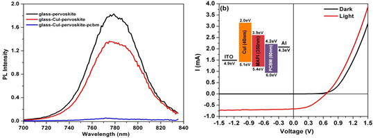
(a) Photoluminescence quenching of MAPI with different active layers. (b) I-V characteristics of fabricated PSC. (Voc= 0.65V, Isc=0.67mA, fill factor =0.41 and PCE=4%.). Inset shows energy level diagram of PSC. |
|
|