|
Major Research Areas
Fundamental physics studies are being pursued with the help of following characterization techniques:
HRXRD measurements
HRXRD studies on Semiconductor Heterostructures
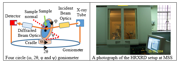
High resolution x-ray diffraction (HRXRD) technique is of paramount importance in device development since it provides a quick and accurate estimate of the crystalline quality of epitaxial layers. However, with the invention of newer combination of layer/substrate materials, it often becomes challenging to acquire and analyze the HRXRD data. In case of mismatch epitaxy, it is indeed a herculean task where the presence of a larger number of defects and dislocations often limits the usefulness of HRXRD technique. HRXRD is preferred due to its non-destructive nature where the crystalline quality of lattice-mismatched epitaxial layers is accessed by measuring the full width at half maximum (FWHM) of Bragg diffraction peaks. In our lab, HRXRD is routinely used by the epitaxial growers for accessing the crystalline quality of layers, which helps them in preparing the next growth recipe rather quickly.
At MSS, HRXRD measurements are performed using a PANalytical X’pert pro MRD diffractometer with a four-crystal Bartels type monochromator for CuK1 radiation providing a beam divergence of 18(12 or 5) arcsec in the scattering plane. An optimization procedure is carried out to orient the tilt and azimuth angles of the Eulerian cradle prior to each measurement. Feedback on the crystalline quality of grown epitaxial structures is an integral step of device fabrication process and the same is routinely carried out in this lab.
Selected publications
-
A simple method to overcome the limitation of hybrid monochromator in the identification of peaks in the HRXRD pattern of Al0.4Ga0.6N/Al0.6Ga0.4N multi quantum wells, T. K. Sharma, R Kumar, A K Sinha, P Pramanik, S Sen, and A Bhattacharyya, Mat. Sci. & Eng. B 240, 92 (2019).
- On the determination of alloy composition using optical spectroscopy in MOVPE grown InGaN layers on Si(111), Vikash K. Singh, Payal Taya, Dipankar Jana, Renu Tyagi, S. Raghavan, T. K. Sharma, Superlattices and Microstructures 134, 106234 (2019).
- R. Kumar, V. K. Dixit, C. Mukherjee and T. K. Sharma, “Anisotropic distribution of microstructure in compressively strained InP/GaAs epitaxial layers”, Superlattices and Microstructure, 122, 636 (2018)
- R. Kumar, V. K. Dixit, and T. K. Sharma, “Anisotropic distribution of dislocations density in tensile strained GaP/GaAs epilayers”, Vacuum 154, 214 (2018).
- Ravi Kumar, V. K. Dixit, Tapas Ganguli, C. Mukherjee, A. K. Srivastava, and T. K. Sharma, "Observation of anisotropic distribution of microstructure in GaP/GaAs epitaxial layers", J. Appl. Phys. 120, 135307 (2016).
|