| Materials Science Section |
|
Major Research Areas
Fundamental physics studies are being pursued with the help of following characterization techniques:
Spectroscopy measurements
Spectroscopy studies on Semiconductor Quantum Structures
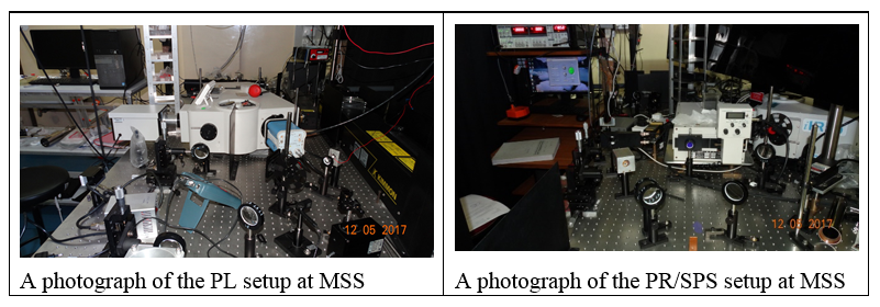
At MSS, fundamental physics studies on epitaxially grown Semiconductor Quantum Structures are carried out with the help of various in-depth spectroscopy measurements. A multiple spectroscopy setup has been indigenously developed where we regularly perform several spectroscopic measurements like photoluminescence (PL), photoluminescence excitation (PLE), photo-reflectance (PR), contactless electroreflectance (CER), photoconducting and surface photovoltage spectroscopy (SPS). Feedback on the optical quality of grown epitaxial structures is an integral part of device fabrication process and the same is routinely carried out in this lab.
PL spectroscopy is a useful technique for the characterization of materials and the dynamical process occurring in materials. PLE technique provides the absorption spectrum of a sample with extremely small absorption, which is not possible in traditional absorption spectroscopy. The same information can also be obtained from PR spectroscopy which is a modulation technique that yields sharp spectral features near the critical points in band structure, thus leading to an accurate determination of the material parameters. SPS can also provide similar information which has been extensively utilized in our group in many applications. A novel dual color SPS technique has been invented by our group which has been proven to quite useful in the investigation of defect related features in nitride epitaxial layers.
Selected publications
-
Confirmation of the compensation of unintentional donors in AlGaN/GaN HEMT structures by Mg-doping during initial growth of GaN buffer layer, Dipankar Jana, Abhishek Chatterjee, T. K. Sharma, J. Lumin. 219, 116904 (2020).
- On the determination of alloy composition using optical spectroscopy in MOVPE grown InGaN layers on Si(111), Vikash K. Singh, Payal Taya, Dipankar Jana, Renu Tyagi, S. Raghavan, T. K. Sharma, Superlattices and Microstructures 134, 106234 (2019).
- Identification of the spatial location of deep trap states in AlGaN/GaN heterostructures by Surface Photovoltage Spectroscopy, Dipankar Jana, S. Porwal, and T. K. Sharma, Superlattice & Microstructure 112, 249 (2017).
- A correlation between the defect states and yellow luminescence in AlGaN/GaN heterostructures, Dipankar Jana, and T. K. Sharma, J. Appl. Phys. 122, 035101 (2017).
- An unambiguous identification of 2D electron gas features in the photoluminescence spectrum of AlGaN/GaN heterostructures, Dipankar Jana and T. K. Sharma, J. Phys. D. Appl. Phys. 49, 265107 (2016).
|
|