Rare earth oxides as gate dielectric for MOS devices
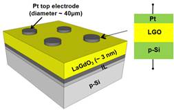
In order to maintain the exponential growth of processing speed and component density, the feature sizes of metal-oxide-semiconductor (MOS) structures in logic devices and metal-insulator-metal (MIM) capacitors in memory devices are down scaled from one technology node to the other following Moore's Law. According to the International Technology Roadmap for Semiconductors (ITRS) Process Integration, Devices, and Structures 2 (PIDS2) table for future high performance logic technology devices (based on extended planar bulk), an equivalent oxide thickness of 6.5 Å is required for 20 nm and below technology node. The urgency and importance of this issue demands that new alternative materials with higher dielectric constants (k>20), large bandgap in ultrathin film form, reduced loss tangent, and lower leakage currents should be developed to achieve long term goal. Recent studies by both academia and industry showed that rare-earth based multi-component oxides in the amorphous state are among the promising candidates for that purpose. We have used optimized pulsed laser deposition to grow amorphous ultra-thin films of ternary interlanthenide oxides LaGdO3, SmGdO3 with dielectric constant > 20 and LaLuO3 with dielectric constant > 30 and studied their electrical properties for advanced gate dielectric applications. To grow Pt/ LaGdO3/Si n-MOS devices, about 50 nm thin Pt gate metal electrodes of area ~ 2.5×105 cm2 were deposited using dc sputtering at a power density of ~ 1W/cm2 through square metal shadow. These devices were passivated using forming gas annealing treatment (90% N2 + 10% H2) at 400 °C for 20 min in rapid thermal annealing (RTA) chamber to reduce the interface trap density. Schematic of Pt/ LaGdO3/p-Si n-MOS devices is shown in figure below (left).
 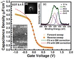
(left) Schematic of Pt/LGO/p-Si n-MOS devices; (right) C-V characteristics of MOS deice measured at 100kHz including its Hauser fit along with (a) Selective area electron diffraction (SAED) image of a-LGO. (b) Cross-sectional TEM images of LGO thin film (c) XPS O1s peak of LGO layer on Si.
The high frequency C-V curve of Pt/ LaGdO3/p-Si MOS devices containing ultra-thin film of LaGdO3 (LGO) having thickness ~ 3 nm is shown in figure (left). It can be seen that C-V characteristics of device is unsaturated (due to ultra-thinness) but close to ideal C-V curve with negligibly small hysteresis. The EOT determined from the accumulation capacitance with and without quantum mechanical correction were ~ 5.4 Å and 8.4 Å respectively which is suitable for practical device application. Cross sectional image of the heterostructures studied using high resolution TEM revealed a ~ 6 Å thin structure less interface layer IL between LGO layer and Si substrate. The XPS measurements confirmed formation of La-Gd silicates and SiOx at interface. The SAED image without any sharp rings or spots revealed amorphous nature of LGO layer. Analysis of temperature dependent leakage currents revealed that gate injection current was dominated by Schottky emission below 1.2 MV/cm and quantum mechanical tunneling above this field. Our studies clearly revealed that LGO could be a promising candidate for the future sub-nanometer logic technology nodes, especially with gate last sequence, by incorporating high-aspect ratio geometries. Further efforts in this direction and on other mixed rare earth oxides are underway.
Other than rare earth mixed oxides we are also involved in exploring binary oxide TiO2 and its multilayers with wide bandgap oxide MgO and Al2O3 for gate dielectric applications. In this direction we have studied the electrical properties for TiO2 based MOS devices where TiO2 thin layer was deposited using optimized pulsed laser deposition. Brief results of this study is presented below
2. TiO2 thin film for MOS devices
We have used PLD to grow pinhole free TiO2 thin films for gate dielectric applications. Metal–TiO2–SiO2–Si (MTOS) capacitors with equivalent dielectric thickness (EDT) in the range of 3.6–13 nm were grown. It has been observed that even though an additional TiO2 layer has been deposited, the capacitance of the MTOS structure actually increases or remains almost the same compared to the MOS device having the same SiO2 layer thickness. Secondary ion mass spectrometric (SIMS) analysis reveals that there is substantial penetration of titanium into the underlying SiO2 layer resulting in a reduction of EDT. In addition, the leakage current of the MTOS capacitor reduced by almost two orders of magnitude and the breakdown field strength nearly doubled after incorporating the TiO2 layer. Thus, PLD is shown to be a viable technique for controlled deposition of TiO2 to achieve lower EDT with smaller leakage current, the two most desirable parameters in present-day MOS devices.
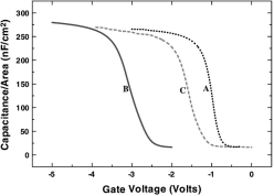 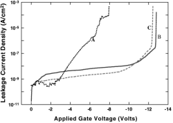
(Left) C–V and (Right) J–V characteristics of reference MOS (curve A), MTOS1 (curve B) and MTOS2 (curve C) capacitors
2.1 Atomic layer deposition of TiO2 thin films
In recent years, atomic layer deposition (ALD) which is a particularly attractive technique in microelectronics manufacturing has received considerable interest within the scientific community to grow TiO2 on planar and high aspect ratio substrates. Due to the high reactivity of the precursors, ALD is frequently used to grow thin films at very low temperatures compared to the other conventional thin film deposition techniques. ALD offers many other advantages like easy and precise thickness control over large deposition area, excellent conformal coating capability on complex-shaped structures, pinhole free dense coatings, no line-of-sight depositions etc. We have used ALD to grow TiO2 thin films under different conditions and studied their structural, morphological, optical and electrical properties for gate dielectric applications
In this study, the TiO2 thin films were grown by ALD in a wide range of substrate temperature varying from ~ 50 to 4000C. The films grown on Si (100) substrates at and below ~ 150 0C were found to be amorphous with quite smooth surface morphologies. However, pronounced RMS surface roughness ~ 29 nm was measured at ~ 200 0C due to the formation of large-size, loosely-packed crystalline grains (mean size ~ 300 nm) oriented parallel to the anatase (101) direction. The atomic force microscopy measurements revealed columnar growths of crystalline grains separated by micron size voids which completely violated the idealized layer-by-layer growth of ALD. With further increment in growth temperature, the nucleation density at the initial stage of film growth was found to be increased which resulted in nanocrystalline densely-packed grains (mean size ~ 40 nm) at and above ~300 0C. The film grown at the highest deposition temperature of ~ 400 0C was found to be composed of both anatase (101) and rutile (110) phases.
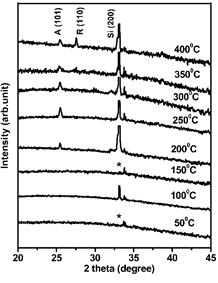 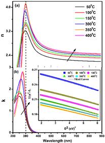
(left) XRD patterns for TiO2 thin films grown on Si (100) substrates at different substrate temperatures (~ 50-400 0C). At the (*) marked positions the Si (200) peak did not appear, (right) Plots of (a) refractive indices and (b) extinction coefficients versus wavelength for the amorphous (grown at ~ 50, 100 and 150 0C) and nanocrystalline films (grown at ~ 300, 350 and 400 0C). The arrows indicate the increase of n and k with increasing growth temperature. The inset of (b) shows plots of 1/(n2-1) versus E2 for the below band-edge refractive indices n as obtained from the single oscillator TL model. The solid lines are their linear fits to the single oscillator WD model.
The refractive index, as obtained from the spectroscopic ellipsometry (SE) measurements was found to be increased from amorphous to the nanocrystalline films. The dispersions of refractive indices below the interband absorption edge as obtained using single oscillator Tauc-Lorentz model were found to be strongly correlated with the single oscillator Wemple-DiDomenico (WD) model. The dispersion energy parameter in WD model was found to be increased from disordered amorphous to the more ordered nanocrystalline films, implied increase in the film density and coordination number. The detailed electrical and dielectric characterizations of the ALD grown TiO2 are underway.
References:
- S. P. Pavunny et al., Properties of the new electronic device material LaGdO3, Physica Status Solidi (b), 251(1), 2014, 131-139.
- S. P. Pavunny et al., Advanced high-k dielectric a-LaGdO3 based high density MIM capacitors with subnanometer capacitance equivalent thickness, Appl. Phys. Lett. 102(25), 2013, 252905.
- D. Saha et al., Spectroscopic ellipsometry characterization of amorphous and crystalline TiO2 thin films grown by atomic layer deposition at different temperatures, , Appl. Surf. Sci. 315, 2014, 116–123.
- S. P. Pavunny et al., Analysis of Leakage Currents through PLD Grown Ultrathin a-LaGdO3 Based High-k Metal Gate Devices, MRS Proceedings, 1561(5-8), 2013.
- S. P. Pavunny et al.,, Advanced high-k gate dielectric amorphous LaGdO3 gated metal-oxide-semiconductor devices with sub-nanometer equivalent oxide thickness; Applied Physics Letters, 102(19), 2013, 192904.
- R. Singh et al., Optimized Dual Temperature Pulsed Laser Deposition of TiO2 to Realize MTOS (Metal- TiO2- SiO2-Si) Capacitor with Ultrathin Gate Dielectric, Semiconductor Sci. Technol. 20(1), 2005, 38-43.
- R. Singh et al., Laser Induced Oxidation of Si for Growth of Ultrathin Gate Oxide, Electronics Letters 40(25), 2004, 1 – 2.
- R. Paily et al., Pulsed Laser Deposition of TiO2 for MTOS Gate Dielectric, Appl. Surf. Sci. 187(3-4), 2002, 297-304.
|