|
Currently ZnO is one of the most sought after semiconductors for developing blue and ultra-violet (UV) Photonic and Spin-Photonic devices such as light-emitting diodes (LED) and laser diodes, Spin-LED, solar blind UV photo detectors, transparent electronic devices and solar cells etc. In bulk, ZnO has a wide and direct band gap of ~ 3.3 eV at room temperature with remarkably high excitonic binding energy which is ~ 60 meV and a rugged chemical and crystalline structure. We have gown device grade thin films of ZnO and its alloy MgZnO and CdZnO using optimized pulsed laser deposition technique and studied their structural, optical and transport properties suitable for optoelectronic device applications. Review of important results is presented below:
-
Buffer assisted growth methodology for ZnO
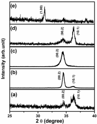
Highly crystalline and epitaxial ZnO thin films were grown by using a novel in-house developed buffer assisted PLD methodology. This methodology envisages growth of thin buffer layer of ZnO at high temperature followed by growth of thick ZnO layer at low temperature. The high temperature buffer layer acts as template layer for over grown ZnO layer and helps in achieving desired in-plane and out of plane orientations with respect to Sapphire substrates which was not possible otherwise. Figure below show Φ-scans, ω-2θ scan, and ω scan of ZnO thin films grown using buffer assisted PLD methodology.
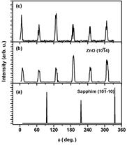
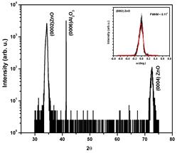
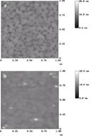
(Left) Φ-scans of (a) Sapphire (b) 50 nm thick ZnO buffer layer grown at 750 °C (c) 200 nm thick ZnO over layer grown at 400 oC, (middle) ω-2θ X-ray diffraction pattern of ZnO thin film grown on (0001) Sapphire and (right) Atomic force micrograph of (a) ZnO buffer layer grown at 750 °C and (b) ZnO over layer grown at 400°C over high temperature buffer layer.
Photoluminescence characteristics of epitaxial ZnO film
Photoluminescence processes in the PLD grown ZnO thin film was studied in the broad temperature range of 10 to 300K to understand various recombination mechanisms and their relative influence on light emission. Temperature dependent recombination from donor bound excitons (BX), free excitons (FX) and their longitudinal optical (LO) phonon replicas were observed. The separation between the FX and BX peak positions was found to reduce with increasing temperature, which was attributed to the transformation of BX into the shallower donor bound exciton complexes at consecutive lower energy states with increasing temperature. The energy separation between the free exciton peak and its corresponding LO phonon replicas showed strong dependence on temperature than that of their bound counterparts. The observed temperature dependence of the energy separation between the free exciton and it’s LO phonon replicas were explained by considering the contribution of kinetic energy to free exciton. The optical properties of PLD grown ZnO was found to be suitable for optolectronic applications.
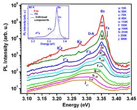 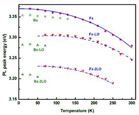
(Left) Photoluminescence spectra of ZnO thin film taken at different temperatures (a) 10, (b) 50, (c) 70, (d) 90, (e) 110, (f) 150, (g) 190, (h) 210, (i) 250 and (j) 300K. The spectra are plotted in logarithm scale, multiplied and vertically displaced for clarity. Inset shows the fitting procedure (solid line) for 90K PL spectrum using Gaussian components shown by dotted lines, (Right) Temperature dependence of energy positions of FX, BX, F/X, B/X, F//X and B//X peaks. Solid line shows the fit to the FX peak values according to Varshani’s empirical relation
-
Atomic Layer Deposition of ZnO
High quality ZnO thin films have been successfully grown by ALD using DEZ and deionized water as metal precursor and oxidant respectively. The ALD window was obtained in the temperature range from ~ 140-200 0C. The ALD grown ZnO films were found to be textured with smooth surface morphology. The ZnO film grown at and above ~ 1850C was found to be polycrystalline in nature with a preferred (00.2) orientation whereas the films grown below 1850C shows a preferred (10.1) orientation. All the films showed excitonic NBE inUV spectral region. The films grown at lower substrate temperatures showed a DLE peak centred at ~590 nm (orange) which was attributed to the presence of additional oxygen related defects in ZnO. The position of DLE peak shifted to ~510 nm (green) at higher growth temperatures due to presence of oxygen vacancy related point defects which were also confirmed by XPS measurements. The films deposited at low substrate temperatures i.e., below ALD window were highly resistive which was attributed to the presence of additional oxygen related point defects in ZnO either in the form of OH groups and/or oxygen interstitials which act as acceptors for the free carriers and/or compensating the existingn-type carriers. ALD ZnO films grown at high substrate temperatures were n-type conducting perhaps due to more complete reactions of the precursors and reduced additional oxygen related defects.
 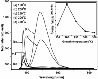
XRD pattern (left) and room temperature photoluminescence spectra (right) of ALD-grown ZnO thin films on (0001) sapphire substrate at different growth temperatures. Inset shows the ratio of intensities of NBE to DLE peaks (INBE/IDLE) as a function of growth temperature.
References:
- P. Misra et al., Buffer Assisted Low Temperature Growth of High Crystalline Quality ZnO Films using Pulsed Laser Deposition, Thin Solid Films, 485(1-2), 2015, 42-46.
- P. Misra et al., Temperature Dependent Photoluminescence Processes in ZnO Thin Films Grown on Sapphire by Pulsed Laser Deposition, Current Applied Physics, 9(1), 2009, 179 – 183.
- D. Saha et al., Studies on optical and electrical characteristics of ZnO thin films grown by atomic layer deposition, Journal Physics Express 3:9 (2013)
- D. Saha et al., Effect of disorder on carrier transport in ZnO thin films grown by atomic layer deposition at different temperatures, J. Appl. Phys. 114 (4), 2013, 043703.
- Amit K. Das et al., Studies on highly resistive ZnO thin films grown by DC-discharge-assisted pulsed laser deposition, Appl. Phys. A, Materials Science & Processing 114 (4), 2014, 1119-1128.
- Kamakhya Prakash Misra, Polarization Characteristics Variation of Visible Light on Reflection from ZnO Based Amorphous Films, Jpn. J. Appl. Phys. 49, 2010, 062602.
- S. M. Jejurikar et al., Structural, morphological and electrical characterization of hetroepitaxial ZnO thin films deposited on Si (100) by pulsed laser deposition: Effect of annealing (800ºC) in air, J. Appl. Phys. 99, 2006, 14907:1 - 7.
- S. D. Singh et al., Synchrotron based photoemission study on the band alignment and interface at ZnO/GaP hetero-junction, Appl. Phys. Lett. 104 (1), 2014, 012109.
- K. Ramamoorthy et al., Development of a novel high speed (electron-mobility) epi-n-ZnO thin films by L-MBE for III–V opto-electronic devices, Current Applied Physics 4 (6), 2004, 679-684.
- K. Ramamoorthy et al., Epi-n-IZO thin films on (100) Si, GaAs and InP by L-MBE – a novel feasibility study for SIS type solar cells, Solar Energy, 77(2), 2004, 193-201
|