|
Research Highlights
b. Recent Publications in Int. Journals.
1. Signature of linear-in-k Dresselhaus splitting in the spin relaxation
of X-valley electrons in indirect band gap AlGaAs
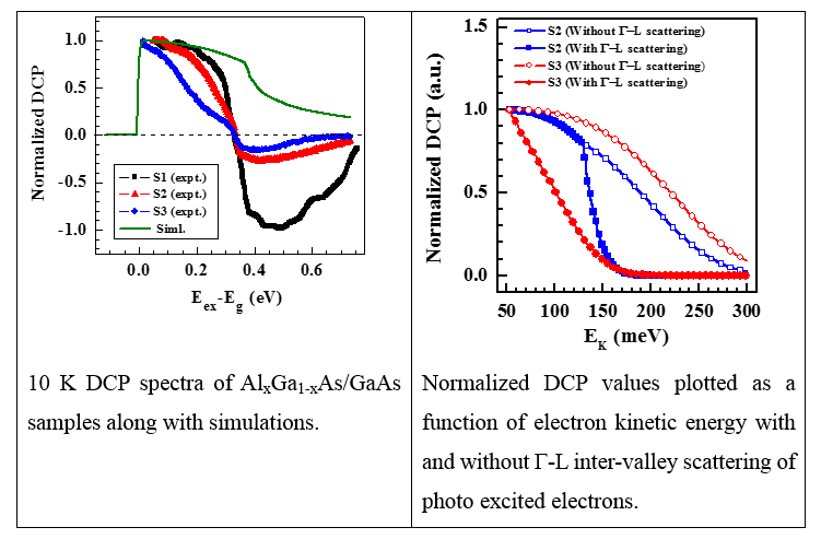
GaAs/AlGaAs quantum well (QW) system is utilized to investigate the electron spin relaxation in the satellite X-valley of indirect band gap Al0.63Ga0.37As epitaxial layers through polarization resolved photo-luminescence excitation spectroscopy. Solving the rate equations, steady state electronic distribution in various valleys of AlxGa1-xAs is estimated against continuous photo carrier generation and an expression for the degree of circular polarization (DCP) of photoluminescence coming from the adjacent quantum well (QW) is derived. Amalgamating the experimental results with analytical expressions, the X-valley electron spin relaxation time (τ_S^X) is determined to be 2.7 ± 0.1 ps at 10 K. To crosscheck its validity, theoretical calculations are performed based on Density Functional Theory within the framework of the projector augmented wave method, which support the experimental result quite well. Further, temperature dependence of τ_S^X is studied over 10-80 K range, which is explained by considering the intra-valley scattering of carriers and Dyakonov-Perel spin relaxation in the X-valley of indirect band gap AlGaAs barrier layer. It is learnt that the strain induced modification of band structure lifts the degeneracy in X-valley, which dominates the electron spin relaxation below 50 K. Furthermore, the DCP spectra of hot electrons in indirect band gap AlGaAs layers is found to be significantly different compared to that of direct bandgap AlGaAs. It is understood as a consequence of linear k dependent Dresselhaus spin splitting and faster energy relaxation procedure in the X-valley.
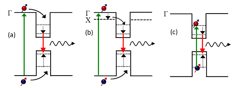
Schematic diagram of electron capture and recombination in AlGaAs/GaAs Quantum Well (QW) for photo excitation in the (a) direct band gap barrier (b) indirect band gap barrier, (c) QW.
Priyabrata Mudi, S. K. Khamari, J. Bhattacharya, A. Chakrabarti, and Tarun K. Sharma
J. Phys. Rev. B. 104, 115202 (2021)
2. Contribution of inter-valley scattering in governing the steady state optical spin orientation in AlxGa1-xAs
Impact of inter-valley scattering in modifying the density of optically injected spin polarized electrons in AlxGa1-xAs/GaAs heterostructure is investigated. Polarization resolved photoluminescence excitation measurements are performed for studying the spectral dependence of degree of circular polarization (DCP) of photoluminescence (PL) signal emanating from an adjacent quantum well (QW) layer. The experimental DCP spectra is found to deviate from the theoretically calculated curve at high excitation energy and the deviation is seen to widen with the Al-content of AlxGa1-xAs barrier layer. In past, researchers had attributed similar deviations to Dyakonov-Perel (D-P) spin relaxation mechanism which dominates the electrons spin dynamics at high excitation energy. However, we find that the inter-valley scattering along with the D-P mechanism decide the shape of optical spin orientation spectra at higher energy. In fact, at higher Al-content, the inter-valley scattering in AlxGa1-xAs layer becomes the most dominant mechanism to govern the steady state electron spin polarization at the band edge. A numerical model is also proposed for estimating the steady state electron spin polarization at zone center by including the inter-valley scattering, energy relaxation and D-P spin relaxation mechanisms.
Priyabrata Mudi, Shailesh K. Khamari, and Tarun K. Sharma Phys. Stat. Sol. RRL
J. Phys. D: Appl. Phys. 54, 495107 (2021)
3. Prediction of inverse spin Hall devices based on the direct injection of carriers in L-valley of GaAs
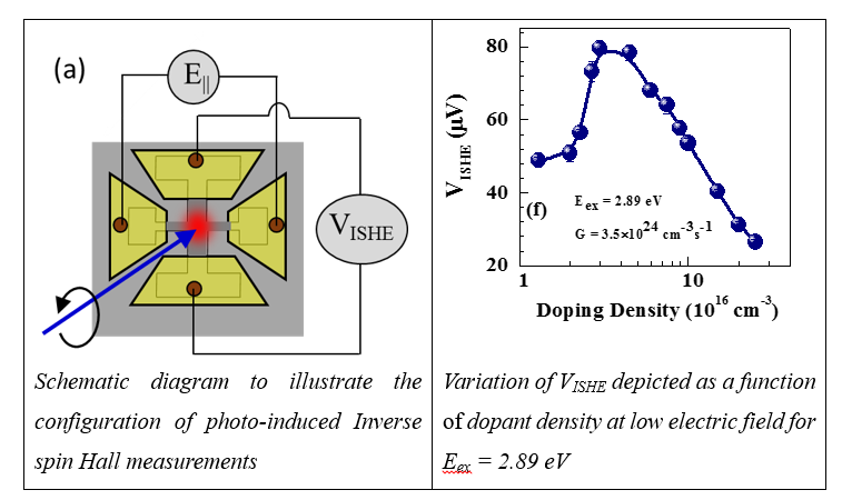
1Numerical simulations are carried out to estimate the Inverse Spin Hall voltage (VISHE) as a function of applied electric field, dopant density and excitation energy for n-GaAs based opto-spintronic devices. Adopting a three valley rate equation model, an expression is derived for the density of spin polarized electrons accumulated in different valleys of conduction band. It is noted that an external electric field can be used to enhance the magnitude of VISHE significantly, however the shape of curve depends upon the choice of excitation energy. A significant rise of VISHE is noted beyond a critical value of electric field when the carriers are injected into -valley of GaAs. On the other hand, a peak like behaviour is observed when hot electrons are injected into -valley. A dual slope behaviour of VISHE with applied electric field is noticed when carriers are injected directly into L-valley of GaAs, where a reasonable value of VISHE can be predicted even for a modest value of electric field. Further, a peak like behaviour of VISHE with dopant density is predicted irrespective of the choice of excitation energy. The optimum dopant density of n-GaAs based Inverse spin Hall devices is found to be ~4×1016 cm-3. Theoretical predictions made in this work are critically important for the realization of next generation Inverse spin Hall devices involving L-valley electrons.
Priyabrata Mudi, Shailesh K. Khamari, and Tarun K. Sharma Phys. Stat. Sol. RRL
J. Phys. D: Appl. Phys. 54, 205101 (2021)
4. Effect of germanium auto-diffusion on the bond lengths of Ga and P atoms in GaP/Ge(111) investigated by using X-ray absorption spectroscopy
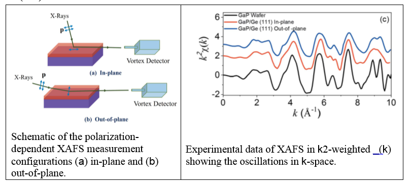
The germanium auto-diffusion effects on the inter-atomic distance between the nearest neighbors of the Ga atom in GaP epilayers are investigated using high resolution X-ray diffraction (HRXRD) and X-ray absorption spectroscopy. The GaP layers grown on Ge (111) are structurally coherent and relaxed but they show the presence of residual strain which is attributed to the auto-diffusion of Ge from the results of secondary ion mass spectrometry and electrochemical capacitance voltage measurements. Subsequently, the inter-atomic distances between the nearest neighbors of Ga atom in GaP are determined from X-ray absorption fine-structure spectra performed at the Ga K-edge. The estimated local bond lengths of Ga with its first and second nearest neighbors show asymmetric variation for the in-plane and out-of-plane direction of GaP/ Ge(111). The magnitude and direction of in-plane and out-of-plane microscopic residual strain present in the GaP/Ge are calculated from the difference in bond lengths which explains the presence of macroscopic residual tensile strain estimated from HRXRD. Modified nearest neighbor configurations of Ga in the auto-diffused GaP epilayer are proposed for new possibilities within the GaP/Ge hetero-structure, such as the conversion from indirect to direct band structures and engineering the tensile strain quantum dot structures on (111) surfaces.
 R. Roychowdhury, P. Rajput, S. Kumar, R. Kumar, A. Bose, S. N. Jha, T. K. Sharma and V. K. Dixit,
J. Synchrotron Rad. 28, 480 (2021)
R. Roychowdhury, P. Rajput, S. Kumar, R. Kumar, A. Bose, S. N. Jha, T. K. Sharma and V. K. Dixit,
J. Synchrotron Rad. 28, 480 (2021)
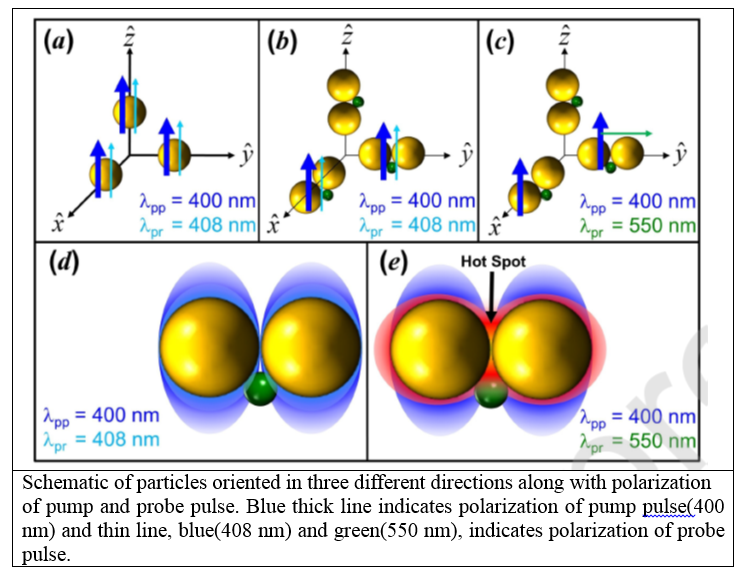
5. Static and Ultrafast Optical Response of Two Metal Nanoparticles Glued
with a Semiconductor Quantum Dot
A hot-spot of high local field can be created between two closely placed metal nanoparticles and by irradiating them with an appropriate wavelength and polarization of incident light. The strength of the field at the gap between the particles is expected to get enhanced by several orders of magnitude higher than that of the applied field. Placing a semiconductor quantum dot or an analyte molecule at the hot-spot is an essential step towards harnessing the enhanced field for various applications. This article shows that it is possible to position a CdTe quantum dot (QD) between two larger silver nanospheres in a colloidal solution. The extinction spectra measured during growth suggests that the final hybrid nanostructure have two touching Ag nanoparticles (NPs) and a CdTe QD in between them close to the point of contact. Using ultrafast transient measurements, it has been shown that the presence of CdTe QD strongly influences the dynamics when the probe excites the gap plasmon. The method demonstrated here to place the semiconductor QD in between the two Ag NPs is an important step in the area of colloidal self-assembly and for the applications of hot-spot in plasmonic sensing, optoelectronics, energy-harvesting, nanolithography and optical nano-antennas.
 S. Gurung, A. Singh, D. P. Khatua, H. Srivastava, and J. Jayabalan
Photonics Nanostructures: Fundam. Appl. 43, 100869 (2021)
S. Gurung, A. Singh, D. P. Khatua, H. Srivastava, and J. Jayabalan
Photonics Nanostructures: Fundam. Appl. 43, 100869 (2021)
|