|
Significant changes in the properties of the nanosized materials compared to their bulk form
primarily derive from the confinement of electrons, phonons and increased surface-to-volume
ratio. Raman spectroscopy being a local probe is extremely sensitive to the material
composition, size, structure, stress, electron-phonon coupling, crystalline quality, local
environment etc., and has become a go-to technique for may researchers across the world for
obtaining new insights into various nanomaterials. Furthermore, the Raman spectroscopy in
conjunction with scanning probe microscopy allows materials reserachers to obtain
correlation between vibrational attributes and surface topology, thus opening new doors in
the understanding of nanostructured materials.
The objective of Raman spectroscopy Lab at RRCAT is to use optical and scanning probe
microscopies together to study optical, electronic, vibrational and electrical properties of
micro/nanostructured materials and correlate them with their morphology for obtaining
important information on them. The understanding developed will open pathways for the
optimization of growth process and timely & non-destructive evaluation of technologically
important materials for device fabrication.
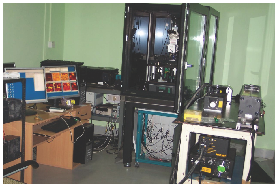
Figure: Scanning probe microscopy (SPM) integrated Raman spectroscopy system
Recent Activities and achievements
(1) Angle-resolved polarized Raman spectroscopy to ascertain the nature/relative
contribution of defects in GaP/Group-IV hetero-structures grown under different
nucleation kinetics
High quality epitaxial structures of compound semiconductors on group-IV (Si, Ge) is the
key for the development of high efficiency multijunction solar cells, wide range of detectors,
lasers and spin-photonic devices. However, it is reported that growth of high quality III–V
polar semiconductor on non-polar substrate, inevitably suffers from hetero-polar interface,
lattice mismatch, diffusion along the interface, etc. These complexities give rise interfaceoriginated
defect structures. Surface nucleation and adatom kinetics play a vital role in
controlling the evolution of structural defects at polar/non-polar GaP/Si,Ge interface, and
their propagation in the overgrowth layer. Therefore, the systematic investigation of
GaP/Si(001) overgrowth layers grown under different nucleation kinetics e.g., Tn1 ~425ºC,
Tn2 ~525ºC and Tn3 ~770ºC (under same flux ratio), is performed by azimuthal angledependent
polarized Raman spectroscopy. Raman measurements infer that intermediate
nucleation (~525ºC) results in high-quality epilayers having substantial suppression of defectexposed
facets. However, the nucleation sites created at high-temperature (~770ºC) give rise
to high-density of defect-mediated non-(001) facets in overgrown layer. The study
demonstrates that the controlled adsorption and optimal mobility of gallium and phosphorous
adatoms at intermediate nucleation temperature (~525ºC) results in superior-quality
overgrowth layers. The proposed methodology serves as quick feedback to determine the
optimized growth kinetics in the given temperature range and hence the efficient integration
of III-V compound semiconductors on Si platform.
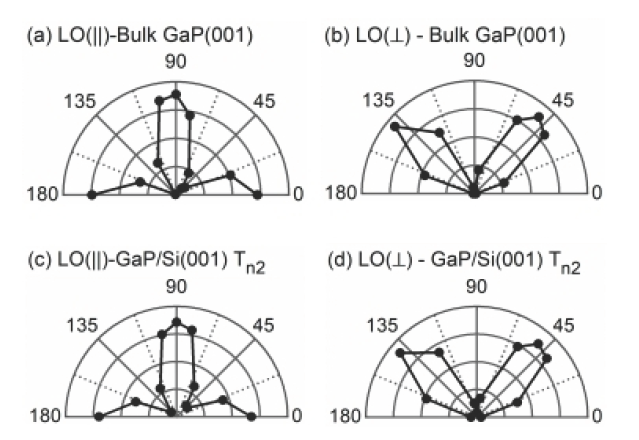
Fig. 1.1. Polar Raman dependence of longitudinal optical (LO) phonon of (a-b) bulk GaP(001)
and (c-d) GaP/Si(001) epilayer grown under intermediate nucleation kinetics Tn2 ~525ºC in
parallel (ei||es) and perpendicular (ei⊥ es) polarization configurations. Polar plots of
GaP/Si(001) layer grown under intermediate nucleation closely mimic the azimuthal patterns of
bulk GaP(001). In the given temperature range, the intermediate nucleation temperature give
rise to best-quality overgrowth layer.
(2) Elucidating the interfacial nucleation of higher-index defect facets in technologically
important GaP/Si(001) by azimuthal angle-resolved polarized Raman spectroscopy
Structural complexities evolving at hetero-polar interface of III-V/Si have been critical
obstacles to high-quality and cost-effective epitaxial integration of wide-bandgap GaP on
closely lattice-matched Si. Unveiling the nature of interfacial defects is quintessential for
efficient integration of III-V semiconductors on Si. Herein. the influence of substrate
crystallographic orientation and therefore the surface energy on the structural properties of
grown layer is explored by investigating the epitaxy of non-polar GaP on extensively used
(001) oriented Si substrate orientation i.e., closely lattice-matched GaP/Si(001) heterostructures.
Polar Raman measurements on GaP/Si(001) hetero-structures reveal that
interfacial nucleation and subsequent coalescence of faceted epiltaxial micro/nano-structures
give rise to higher-index defect-exposed {111} and {112} facets in the overgrowth layer. To
the best of our knowledge, this is first of it’s kind work wherein angle-dependent polarized
Raman measurements are employed for ascertaining the nature and orientations of interfacial
defect facets in advanced hetero-structures.
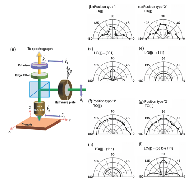
Fig. 2.1 (a) Typical schematic of Raman back-scattering configuration utilized for determining the
azimuthal angle dependence of intensity of optical phonons scattered from a given crystal
orientation. (ei, ki) and (es, ks) are the incident and scattered light polarization and propagation
wave vectors respectively. Observed polar dependence of LO phonon of GaP/Si(001) thick layer
(TL) hetero-structure in parallel (ei||es) polarization configuration arising from spatial position of
(b) type ‘1′ (where peak intensity ratio R = ITO/ILO is less than unity in unpolarized spectra) and (c)
type ‘2′ (where peak intensity ratio R = ITO/ILO is nearly one in unpolarized spectra). Calculated
azimuthal angle dependence of LO phonon for scattering from (d) (001) and (e) (111) plane.
Observed polar plots of forbidden TO phonon of thick layer hetero-structure in parallel
configuration at position of (f) type ‘1′ and (g) type ‘2′ . Calculated TO phonon azimuthal
dependence for scattering from (h) (111) facets and (i) combination of (001) and (111) facets.
Observation of symmetry-forbidden phonon/s and their azimuthal-dependence evidences the
formation defect-mediated {111} and {112} facets.
(3) Investigations on the origin of strain variation in the zinc-blende phase along the
depth of GaP/Si(111) using spatially resolved polarized and wavelength dependent
Raman spectroscopy
The surface and micro structure variations in the technologically important GaP/Si heterostructures
are investigated by the spatially resolved polarized and wavelength dependent
Raman spectroscopy. The hetero-structures probed from two different directions <1 1 1> and
<1 1 0> reveal the presence of strain distributed zinc-blende (ZB) GaP phases along the depth
and the dominance of wurtzite (WZ) phase near the GaP-Si interface. The azimuthal
dependence of the optical phonon intensity of nucleating layer endorses the dominance of
WZ phase at the interface. The study illustrates that spatially resolved polarized Raman
probe, across the hetero-junction is extremely useful for distinguishing the WZ and ZB
stacks. The study bestows with new opportunities for engineering of the GaP/Si based crystal
phase quantum structures with atomically sharp interfaces. The findings illuminate that the
Spatially resolved Raman spectroscopy can serve as a quick and impactful alternative to time
consuming and cumbersome high-resolution transmission electron microscopy / in situ
reflection anisotropy spectroscopy measurements for probing the surface and interface
properties of such hetero-structures.
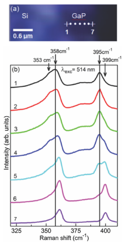
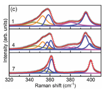
Fig. 3.1. (a) Optical image of cross-sectional surface of GaP/Si(111) thick layer (b) Raman spectra at
seven spatial positions (separated by ~100nm) across the cross-sectional surface marked in (a), and
(c) Deconvolution of contributions to Raman spectra at positions ‘1’, ‘4’ and ‘7’ using minimum
number of Lorentzian and Gaussian lineshapes. E2H (wurtzite), SO and TO/LO (zinc-blende) phonons
contributions are shown in orange, magenta and blue colors, respectively. Red colour is total fit to
data (+). Evolution of Raman spectra from near-interface (position 1) to near surface (position 2)
showcases the strain-gradient zinc-blende phases and wurtzite phase GaP.
(4) Predicting surface modification of InAs nanowires on laser irradiation using
transient thermal simulation and time evolution of Raman spectra
For fine tuning the properties of semiconductor nanowires(NWs), modifications of the
surface and dimensions of these nanowires using laser irradiation are being explored as one
of the methods. In order to control the oxidation processes leading to surface modifications,
one needs to obtain understanding of temperature rise at the surface of NW under laser
irradiation. In this work, we first establish correlation between simulated temperatures at the
surface of a InAs nanowire (NW) with time evolution of Raman spectra, on laser irradiation.
Transient thermal simulations are performed with ANSYS software using finite element
method, considering 3D geometry of the irradiation setup. In the systematic study of laser
irradiation (laser power densities ~ 30-636 kW/cm2) over time duration of ~8 minutes, the
simulated temperature is found to corroborate well with the corresponding oxidation
processes e.g. weak (WP), intermediate (IP) and strong process (SP), occurring on the surface
of InAs nanowire under various laser irradiation conditions. The predictability of the
methodology was then investigated by applying it to random conditions of NW like diameter,
aspect ratio and laser power density etc. for i) NWs found in the same sample and ii) InAs
NWs grown elsewhere and transferred on other Si substrate. The study establishes
predictability of various oxidation processes for given NW dimensions, laser power density
and irradiation time, thus validating the importance of temperature simulation in predicting/
controlling the required surface modification for other III-V NWs useful in nanotechnology.
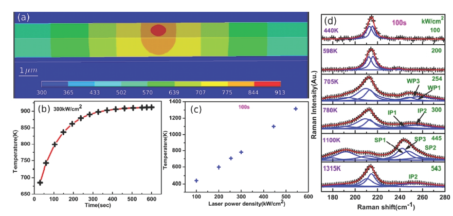
Fig. 4.1. (a) 3D temperature profile (staedy state) (b) Time evolution of simulated temperarture for
InAs nanowire (NW: d~800 nm, L~36 μm) on Si substrate for laser power density (LPD)~300 kW/cm2,
(c) Variation of simulated temperature at 100s as a function of LPDs and (d) Raman spectra with 488
nm at 100s for LPDs. Simulated temperature and oxidation processes for each spectra are noted.
Earlier Achievements/Studies
(1) Co-localized Raman and AFM mapping of Si-SiO2 nanocomposites:
|
Raman spectroscopy monitored laser irradiation
experiment in corroboration with DFT/TDDFT
calculations and X-ray photoelectron spectroscopy
suggests:
(i) Si phonons: 495 - 510 cm-1 originate from the
smaller size (< ~ 4 nm) Si nanocrystals and it’s
frequency is governed by dominant surface/interface
effect.
(ii) Si phonons: 515 - 519 cm-1 originate from larger
size Si nanocrystals (> ~ 6 nm) and it’s frequency is
governed by the confinement effect.
(iii) Si phonons: 511 - 514 cm-1 originate from
intermediate size Si nanocrystals (~ 4 to 6 nm) and
it’s frequency is governed by simultaneous contribution of core and surface.
|
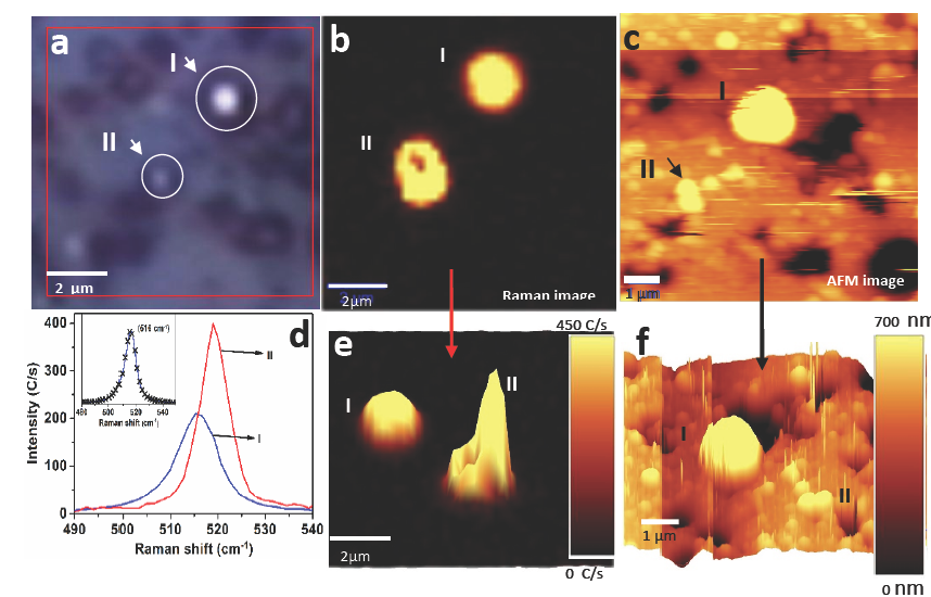
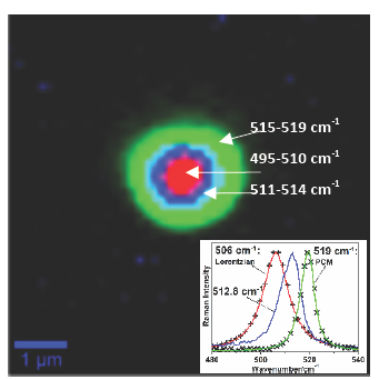
Fig. 1.1. (a) Optical (b) Raman and (c) AFM images of the type I and II Si nanocrystals as depicted in
the pictures, (d) Raman spectra of type I and type II nanocrystals. 3D (e) Raman and (f) AFM images
of the same type I and type II nanocrystals.
The sensitivity of Raman spectroscopy to surface/interface and confinement effects in
nanocrystals is effectively used to correlate Raman mapping with AFM to understand that Si
NCs are clustered in i) smaller clusters (~ 100 nm) organized closely in two dimensions and
ii) big (~ 2 μm) three dimensional isolated clusters.
(2) Raman and atomic force microscopy of CdS nanocrystals grown in PVP matrix
using chemical bath deposition (CBD)
CdS-PVP nanocomposites grown with various concentrations of Cd+/S- and PVP are studied
using Raman and atomic force microscopy mapping on same chosen areas of the sample.
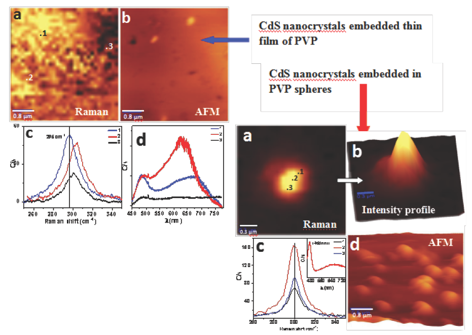
Fig. 2.1. Left side Image: (a) Raman map (b) AFM scan (c) Raman spectra and (d) PL spectra of CdS
nanoscrystals embedded thin film of PVP at three spatial positions marked by ‘1’, ‘2’ and ‘3’. Right side
image: (a) Raman map (b) 3D intensity profile (c) Raman spectra at three spatial positions of CdS
nanoscrystal embedded in PVP sphere, (d) AFM map of the region containing CdS nanocrystals embedded
in PVP spheres.
- CdS nanocrystals are embedded in either a thin-film or spheres of PVP, formation of
which depends on relative ratio of Cd+/S- concentration (density of nanocrystals) to PVP.
- Collapse of PVP from planer matrix to the sphere morphology is correlated with the
interaction between nanocrystals and polymer leading to a co-operative growth
mechanism.
- The stoke-antiStoke ratio, line shape, line width of phonons observed in Raman spectra
gives information of growth mechanism, crystalline quality and confirms presence of CdS
in PVP balls: imaged using CdS: LO phonon peak.
Related Publications
-
V. Gupta, A. A. Ingale and R. Aggarwal, Novel use of selectivity of Resonance Raman
spectroscopy to study polytypism and mixed to pure phase conversion in individual InAs
NWs on laser irradiation, Appl. Surf. Sci. 600, 154091 (2022)
- R. Aggarwal, A. A. Ingale and V. K. Dixit, Elucidating the interfacial nucleation of
higher-index defect facets in technologically important GaP/Si(001) by azimuthal angleresolved
polarized Raman spectroscopy, Appl. Surf. Sci. 554, 149620 (2021)
- R. Aggarwal, Alka A. Ingale and V.K. Dixit, Investigations on the origin of strain
variation in the zinc-blende phase along the depth of GaP/Si(111) using spatially
resolved polarized and wavelength dependent Raman spectroscopy, Appl. Surf. Sci. 514,
145933 (2020)
- R. Aggarwal, Alka A. Ingale, V. K. Dixit and V. Sathe, Raman spectroscopy investigation
of inter-diffusion in GaP/Ge(111) hetero-structures, Superlatt. and Microstruct. 125 190
(2019)
- R. Aggarwal, P. Ram Sankar, A. Sahu, Alka A. Ingale, A. K. Sinha, C. Mukherjee,
Template based room temperature growth of high density CdS nanowires from aqueous
electrolyte using high frequency alternating current, J. of Mater. Sci.: Mater. Electron.
29, 427 (2018)
- V. Gupta, A. A. Ingale, A. Bhattacharya, M. Gokhale, R. Aggarwal, S. Pal,
Understanding the effect of nanowire orientation on time evolution of Raman spectra
from laser irradiated InAs nanowire surface, Nanotechnology, 29, 425709 (2018)
- R. Aggarwal, Alka A.Ingale, V. K. Dixit, Raman spectroscopy and atomic force
microscopy study of interfacial polytypism in GaP/Ge(111) heterostructures, Applied
Surface Science 427, 754-762 (2018)
- Vandna K. Gupta, Alka A. Ingale, Vikas Jain, R. Aggarwal, S. Pal, Predicting surface
modification of InAs nanowires on laser irradiation using transient thermal simulation
and time evolution of Raman spectra, Journal of Alloys and Compounds 735,1331
(2018).
- Ekta Rani, Alka Ingale, D. M. Phase, A. Chaturvedi, C. Mukherjee, M. P. Joshi and L.
M. Kukreja, Band gap tuning in Si-SiO2 nanocomposite: Interplay of confinement effect
and surface/ interface bonding, Applied Surface Science 425C, 1089 (2017).
- Ekta Rani, Alka A Ingale and A K Sinha, Interaction between CdS nanocrystals and PVP
leading to co-operative growth of CdS PVP nanocomposites: A Raman and AFM
mapping study, Journal of Alloys and Compounds 729C, 597 (2017)
- Vandna K. Gupta, Alka A. Ingale, Suparna Pal, R. Aggarwal and V. Sathe, Spatially
resolved Raman spectroscopy study of uniform and tapered InAs micro-nano wires:
Correlation of strain and polytypism, J. Raman spectroscopy 48, 855 (2017).
- Ekta Rani, Alka A. Ingale, A. Chaturvedi, M. P. Joshi and L. M. Kukreja, Corroboration
of Raman and AFM mapping to study Si nanocrystals embedded in SiO2, J. of Alloys
and Compounds 672, 403 (2016).
- Ekta Rani, Rahul Aggarwal, Alka A Ingale, K. Bapna, C. Mukherjee, M. K. Singh, P.
Tiwari and A. K. Srivastava, Insight into one-step growth of nearly monodispersive CdS
nanocrystals embedded in polyvinyl pyrrolidone spheres, J. of Materials Science 51,
1581 (2016).
- Ekta Rani, Alka A. Ingale, A. Chaturvedi, C. Kamal, D. M. Phase, M. P. Joshi, A.
Chakrabarti, A. Banerjee and L. M. Kukreja, Correlation of size and oxygen bonding at
the interface of Si nanocrystal in Si-SiO2 nanocomposite: A Raman mapping study, J. of
Raman Spectroscopy 47, 457 (2016)
- Ekta Rani, Alka A. Ingale, A. Chaturvedi, M. P. Joshi and L. M. Kukreja, Resonance
Raman mapping as a tool to monitor and manipulate Si nanocrystals in Si-SiO2
nanocomposite, Appl. Phys. Lett. 107, 163112 (2015).
- Suparna Pal, R. Aggarwal, Vandna Kumari Gupta and Alka Ingale, Time evolution
studies of laser induced chemical changes in InAs nanowire using Raman spectroscopy,
Appl. Phys. Lett. 105, 012110 (2014).
- R. Aggarwal, Alka A. Ingale, Suparna Pal, V.K. Dixit, T. K. Sharma and S. M. Oak,
Intersubband plasmon-phonon coupling in GaAsP/AlGaAs near surface quantum well,
Appl. Phys. Lett. 102, 181120 (2013).
|


 Home Laser Physics Applications Division


