|
Major Research Areas
Fundamental physics studies are being pursued with the help of following characterization techniques:
Electronic transport measurements
Electronic Transport studies on Semiconductor epitaxial layers
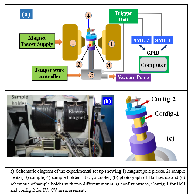
Electronic Transport studies on epitaxial layers are an essential step in the optimization of the performance of semiconductor devices. The measurements like Hall Effect, current-voltage, capacitance-voltage (CV), and admittance spectroscopy are routinely performed in our lab. The characterization procedure includes investigation of mobility and carrier concentration by Hall measurements, whereas leakage current, barrier height and ideality factor are determined by the current-voltage measurements. Further, depth profiling of carrier concentration is performed by CV and ECV techniques. The temperature dependent Hall measurements are performed using two Keithely 236 source/measure units and one 2361 trigger controller unit over a wide temperature range using Helium based close cycle refrigerator. The schematic of electronic transport measurement setup is shown in figure given below. The measurement system consists of an electromagnet providing a static magnetic field with a peak field capability of 1.5 Tesla. For Hall measurements to be performed under van der Pauw geometry, the sample is mounted in config-1 while in config-2 for the CV measurements.
Selected publications
-
Confirmation of the compensation of unintentional donors in AlGaN/GaN HEMT structures by Mg-doping during initial growth of GaN buffer layer, Dipankar Jana, Abhishek Chatterjee, T. K. Sharma, J. Lumin. 219, 116904 (2020).
- Role of ZrO2 Passivation Layer Thickness in the Fabrication of High Responsivity GaN Ultraviolet Photodetectors, Abhishek Chatterjee, Shailesh K. Khamari, S. Porwal and T. K. Sharma, Phys. Status Solidi RRL 13, 1900265 (2019).
- Peculiarities of the current-voltage and capacitance-voltage characteristics of plasma etched GaN and their relevance to n-GaN Schottky photodetectors, Abhishek Chatterjee, V. K. Agnihotri, S. K. Khamari, S. Porwal, A. Bose, S. C. Joshi and T. K. Sharma, J . Appl. Phys. 124, 104504 (2018).
- Effect of 60Co -irradiation on the nature of electronic transport in heavily doped n-type GaN based Schottky photodetectors, Abhishek Chatterjee, S. K. Khamari, S. Porwal, S. Kher, and T. K. Sharma, J. Appl. Phys. 123, 161585 (2018).
- Dislocations limited electronic transport in hydride vapour phase epitaxy grown GaN templates: A word of caution for the epitaxial growers, Abhishek Chatterjee, Shailesh K. Khamari, R. Kumar, V. K. Dixit, S. M. Oak, and T. K. Sharma, Appl. Phys. Lett. 106, 023509 (2015).
|