|
Major Research Areas
R&D on laser diode arrays
Investigation into the complexities in active region of quantum
well laser diode arrays
1. Introduction :
The photonic devices based on III-V
semiconductors started instinctive development after
the invention of the light emitting diode (LED) and laser
diode (LD). Subsequently, in the last five decades LEDs
and LDs remains the cardinal components, both in
traditional and modern applications which includes
telecommunication, data storage & processing, optical
sensors & sensing networks, image processing, high
efficient low power lightening, display & cinema,
materials processing, 3D printing, molecular & bio
photonics etc [1]. Even pioneers in this field report that
the laser diodes are the future for lighting and have
imperative advantages over LED because of higher
efficiency [2]. In spite of numerous applications of these
devices, several newer challenges are also arising, such
as high power with controlled wavelength and low
divergence, wide wavelength tuning for advanced
material processing, monolithic integration on Si and
low threshold high efficiency spin laser [3-7]. The
success secrets of these devices predominantly depends
on the efficient radiative recombination of the carriers
into an optically active region of the forward-biased p-in
junction diode. Fig. 1a shows the schematic of
forward-biased p-i-n junction diode in which the
conduction &valence band edges E , E are plotted as c v
solid lines. The dashed lines represents Fermi energy E , F
that splits into quasi-Fermi energy E and E in the Fc Fv
undoped transition region, where holes and electrons
recomibines. In this region, inversion condition, E - Fc
E > ħ >E can be easily achieved because the quasi- Fv g
Fermi energy are inside the bands. This optically active
region consist of quantum wells (QWs) and by tuning its
structural parameters one can control the properties of
the devices. Thus, in order to meet the newer challenges,
one need to understand the complexities of the materials
used in the QWs. Some of these complexities are
distinguishable under extreme conditions, such as at
very high injection current, the emission wavelength may start shifting to higher wavelength. This is mainly
due to excess internal heating caused by the nonradiative
recombination and the migration of charge
carrier into the localized states and subsequent radiative
recombination via those states. The charge carriers
localized in these states have different effective mass
and therefore can affect the laser diode properties
including the operating wavelength, threshold current
density and electrical to optical conversion efficiency
etc [4, 8]. Thus to meet the present requirements, both
the basic studies on QW and engineering on laser diode
structures are the prime focus of laser diode community.
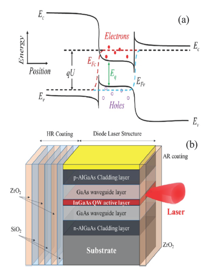
Schematic of laser diode structures grown by
using MOVPE at RRCAT (a) Forward-biased p-i-n
junction (b) Description of multilayer, front & rear
facets coated with single & multilayer stacks of ZrO & 2
ZrO /SiO (not to scale).
The recent investigations on Bragg-like waveguide
resulted an ultra-narrow circular beam for edge emitting
laser diodes[9]. Similarly, investigations on new sets of
multilayer materials ZrO2 and ZrO2/SiO2 used for facet
coting, assured to have increase damage threshold of
these laser diode array[10]. Further, very recent
innovations in QW intermixing and asymmetric
waveguides resulted unique high power, brightness, and
reliability which eliminated the problems associated
with catastrophic optical mirror damage[11]. In India,
in-spite of some early achievements, progress in this
field is slow, both in research &technology front, due to
several limitations and unavailability of semiconductor
resources. In-spite of these facts, we at RRCAT have put
strong efforts & developed high power QW lasers in the
wavelength range of 670 to 1000 nm. The active regions
of these laser diodes mainly consists of AlGaAs/GaAs,
GaAs/InGaAs, & AlGaAs/GaAsP QWs [10, 12-13].
One such QW laser diodes arrays with ~ 980 nm
emission wavelength, delivered 23.5 W peak power
under pulsed operation and 3 W, CW power. However
the operating wavelength shifts towards higher
wavelength with the increase of injection curent. In
order to understand this process and for meeting the
future requirement of the department, we have
investigated the ultralow disorders and effective mass
parameters for these QWs and active region of laser
diode structures using temperature, excitation power
and magnetic field dependent photoluminescence (PL).
Here in this article, we summarise the progress of high
power laser diode arrays development work at RRCAT.
Subsequently, we also discuss the complexities of the
active region of QW laser diode arrays with a particular
aim of the development of fiber lasers.
2. Experimental Details:
The epitaxial structure of semiconductor QWs and
laser diodes are grown on nominally(001) oriented n+-
GaAs substrate (carrier density ~ 1×1018 cm-3) by using
horizontal low-pressure metal organic vapor phase
epitaxy (MOVPE) reactor (AIX-200). Trimethyl
Gallium (TMGa), Trimethyl Indium (TMIn) and
TrimethylAluminium (TMAl) are used as precursors for
group III elements while 100% Arsine (AsH ) is used for 3
group V element. Dimethyl Zinc (DMZn) and 2% SiH 4
in H are used as the dopant source for p- and n-type 2
doping respectively. The single QW structures of
AlGaAs/GaAs, GaAs/InGaAs, InP/InAsP and
AlGaAs/GaAsP are grown and their basic properties are investigated using numerous techniques [10,12-21].
The complete laser diode structures are also grown
which consist of AlGaAs based cladding layer, graded
refractive index layer, waveguide layer and the active
region embedded with double quantum wells of above
materials(Fig.1b). The grown laser diode structures are
processed through conventional optical lithography, nand
p- type metal contact formation by e-beam/thermal
evaporation, lift-off process, and rapid thermal
annealing. After making a smooth walled mesastructure
using H PO :CH OH:H O etchant solution, 3 4 3 2 2
electrical isolation and side-wall passivation is realized
by SiO layer deposition between the metal stripes. 2
Finally, the structure is thinned down to ~140 m and
several laser elements of 500 m cavity length and 100 m
strip width are cleaved. Subsequently, antireflection and
high reflection coatings of ZrO based multilayers are 2
carried out on the laser diodes using e-beam
evaporation. The low deposition temperature is
preferred to avoid any deleterious diffusion of materials
in the active region of laser diodes. Surface and interface
properties of single and multilayer facet coatings of
ZrO and ZrO /SiO are investigated by optical and X- 2 2 2
ray reflectivity (at Indus-1) [10]. Subsequently, the laser
diode characteristics are evaluated in the light output
power versus current (L-I) testing setup that is equipped
with precision pulsed laser diode driver, power meter,
spectrometer, mounting stage, microscope etc. Further,
the die bonding process is optimized with two different
types of solder materials namely Indium preform (soft
solder) and Gold-Tin (AuSn-hard solder). The LD
devices are bonded on gold plated Copper and KOVAR
substrates. Finally, semiconductor laser diode arrays are
die bonded and packaged in a water cooled micro
channel based gold coated assembly. The photographs
of processed laser diode arrays along with gold coated
assembly are shown in Fig.2.
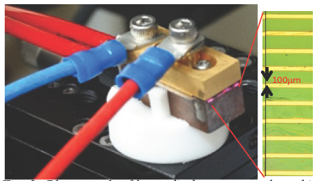
Photograph of laser diode arrays packaged in
the microchannel assembly by RRCAT.
as ultralow disorders and effective mass in the
QWs & LD structures the contactless Magneto-PL
experiments are performed (Fig.3). In this setup, sample
is kept in a holder of variable temperature inserts (VTI)
which is immersed inside a Dewar of the thermostat
where the lowest temperature of 1.2 K with mK
accuracy can be achieved. High magnetic field up to 8T
is achieved by helical shaped niobium-titanium
superconducting magnet. Figure 3(a) show the
photograph of superconducting magnet. The laser light
is passed through band pass filter to remove any
unwanted fluorescence lines from the diode-pumped
solid-state lasers, followed by neutral-density filters to
control the laser excitation power. The laser excitation
power is kept at minimum levels to reduce the intensity
dependent effects, such as saturation of energy levels,
linewidth broadening, temperature rise etc. The
chopped laser light is focused into an optical fiber using
gold coated GaAs mirror.The excitation laser beam is
guided through an optical fiber having ~ 400 μm
diameter with ~ 3 meter length. Samples kept at 1.2K are
excited by the laser light that is guided with the help of a
Magneto-PL setup at RRCAT (a)
Superconducting magnet, (b) PL with fiber coupling, (c)
Electronic controls, (d) Schematic of Magneto-PL
setup.
fiber and the same fiber is used to collect the PL signal.
The PL signal after suitable filters is dispersed by
monochromator and detected by Si/Ge photodiode
using lock-in amplifier technique. Figures 3(b) & (c)
show the optical and electrical data processing
arrangement for magneto-PL experiment. In this
experiment, the sample is mounted horizontally in the
VTI assembly and field is applied along the growth
direction, also the direction of light, known as Faraday
geometry, and excitonic properties are probed in the
plane of the sample, shown in Fig. 3(d). Under this
condition, the magnetic field driven confinement of
charge carrier at high field produce discrete harmonic
oscillator like Landau energy levels which blue shift
with field. From the analysis of PL line width and the
field dependent blue shift microscopic parameters are
obtained. The details are given in next section.
3. Results and Discussion:
A. Structural Analysis and Limitations:
In-depth structural parameters, such as layer
thickness, composition and strain, interface roughness
of the grown structures are determined from high
resolution x-ray diffraction (HRXRD), transmission
electron microscopy (TEM) and x-ray reflectivity
(XRR) by Hard/soft x-ray beam of CuK lab α
source/synchrotron radiation source at Indus-1
synchrotron beamline facility, respectively [10,12-23].
It is concluded from the structural analysis that the
semiconductor heterojunction and quantum structures
are of excellent quality. However, all these techniques
do not predict directly the influence of ultralow disorder
on the opto-electronic properties of the material. In
contrast, contactless PL and surface photo-voltage
(SPV) spectroscopy are more effective techniques for
studying the optical quality and also the defects.
Superiority of these contactless techniques lies in their
simple and non-destructive nature. Localization of
charge carrier and their dynamics can be understood
from the conventional emission and absorption of
photon based PL and SPV techniques.
B. Photo luminescence &Surface Photo Voltage
Analysis:
In order to investigate the emission wavelength
and carrier recombination mechanism in the grown
structures, intensity and temperature dependent PL measurements are performed. PL spectra of several
QWs are shown in Fig.4a. The origin of PL emission is
explained by the theoretically calculated values
obtained by solving the Schrodinger equation using
finite difference approach within an envelope-function
formalism framework[24]. It is observed that for the
same power density of excitation the relative
recombination efficiency of AlGaAs/GaAs QW sample
is high compared to other QW materials.
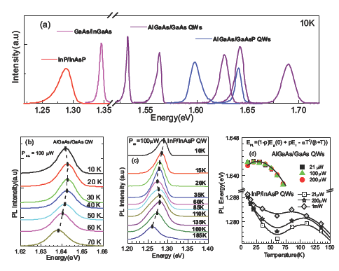
a) 10K PL spectra of QWs, Temperature
dependent PL spectra of QWs b) AlGaAs/GaAs c)
InP/InAsP, Power and temperature dependent energy
band gap variation for AlGaAs/GaAs &InP/InAsP
QWs.
The recombination efficiency variations among
the QW materials may be due the combined effect of
several factors including effective mass, wave function
overlap, influence of atomic irregularity, effect of
barrier layer, different magnitude of photon absorptions
etc. It is also observed that almost all the QW samples
show monotonic decrease in transition energy with rise
in temperature. However at low temperatures, these
samples show different temperature dependent behavior
(Fig 4b & c). This behavior is different for different level
of illumination power (Fig 4d). The samples with
ternary materials in QWs mostly show anomalous S
(red-blue-red) shaped energy versus temperature
behavior, while samples with binary material in the QW
region does not show such behavior. The S-shaped
temperature dependence of ground state transition
energy is explained by considering thecarrier localization in the band-tail states at low temperatures
where the ground state energy follows the temperature
dependence of the localization states. One therefore sees
a normal temperature induced bandgap shrinkage (red
shift) up to the critical temperature which is mainly
governed by the localization energy. At a critical
temperature, excitons having sufficient thermal energy
enabling their delocalization which leads to the
dominance of band to band exciton feature. Because of
this, the energy of ground state feature increases (blue
shift) until the localized exciton feature starts to weaken
upto critical temperature (Fig4d).Above this
temperature, excitons are in thermal equilibrium and
once again one sees the usual temperature induced
bandgap shrinkage (red shift) up to room temperature.
At reasonably high excitation intensities, a large
numbers of electron-hole pairs are generated which lead
to the saturation of band tail states that reduces the effect
of carrier localization because of the limited density of
localized states. Under such condition, though the band
to band recombination dominates over the localized
states recombination but they influence the
luminescence spectra significantly. In such a situation
conventional models of Varshni, Viña and Passler break
down where Dixit et al.[12] have proposed a
phenomenological model for evaluating the material
parameters and localization energy of carriers trapped in
the band-tail states as given below,
where E Peakis the PL peak energy at a given PL
temperature, n and n are the associated weighting 1 2
factors which tells if either the transitions are band-toband
dominated or the localized exciton dominated at
energy E QW(0) and E (0) respectively [12]. Here, F(T) is g t
the temperature dependent term which takes into
account the electron-phonon interaction and thermal
expansion of the lattice parameters. If the fraction (p) is
defined in terms of weighting factors as p= n /(n +n ) 2 1 2
then equation 1 can be rewritten as,
The material parameters (α, β) and localization energy
(ΔE = E QW(0) - E ) for all the QW samples showing such g t
behavior can be obtained. Here, α tells the disorders or
entropy of the system while β is related to Debye or phonon temperature. Thus for ternary QWs system
using above process one can estimate the trap energy
values and materials parameters which can also give
information of disorders in the systems. It is further
explained how the magnitude of charge carrier
localization energy influences the critical temperature
of S-shaped temperature dependent energy variation. It
is also proposed a methodology to extract the value of
carrier localization energy directly from temperature
dependent SPV and PC [12,14-15].This information can
play a pivotal role in defining the operating temperature
range of absorption based quantum structures devices,
where such S-shaped behaviour of excitonic transition
energy is observed.
C. Magneto-PL analysis:
In order to investigate the microscopic properties
of exciton, such as effective mass, binding energy, Bohr
radius and ultralow disorders for semiconductor
quantum structures, contactless Magneto-PL
measurement are performed. In the Faraday geometry,
the excitonic properties are probed in the plane of the
sample. It is observed that the spectrum of all the
samples show blue shift with applied magnetic field due
to the predominant contributions of diamagnetic and
Landau shifts (Fig. 5 a & b). The magnetic field
dependent diamagnetic blue shift of PL spectra is
proportional to the square of B (B <B ) [16]
However, at relatively higher magnetic field, excitons
perform cyclotronic motion, having very small radius
(at B = 8 T radius r ≈ 90.7 Å), being centered on their
center of mass motion. This magnetic field driven
confined motion (in x-y plane) of charge carrier is
responsible for the formation of discrete Landau levels.
In this region (B ≥ Bc), blue shift in energy levels
become proportional to the applied field B [16].

Here, R &r are the dimensionality factor & Bohr radius D B
respectively, &α, β are the proportionality constants. μ*
is the reduced effective mass of exciton and can be
expressed as, 1/μ* = 1/m * +1/m *, with m * &m * are the effective mass of electron &hole, respectively
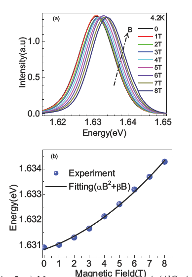
a) Magneto-PL spectra of GaAs/AlGaAsQW b)
Blue shift of PL peak energy as a function of B.
The magnetic field, above which magnetic energy
becomes dominant over Columbic energy, is termed as
critical magnetic field (B = μ*2e3/16π2ε 2ε 2ħ 3), and is c 0 r
theoretically estimated as 4.9 T for GaAs. Here, ε = r
13.18 is the dielectric constant of GaAs, ε is the 0
permittivity of free space and ħ is the (Planck's
constant)/2π. Thereafter, excitonic model is used to
estimate the reduced effective mass of excitons for all
QWs using the Magneto-PL spectra. Significant
increase of effective mass is observed for the confined
exciton in narrow QWs. The foremost reason behind
such an observation is due to the induced nonparabolicity
in bands, which varies with the thickness of
the QWs [16]. In order to obtain such results on the laser
diode structure, we have performed similar experiment
and observed interesting results which are discussed
below.
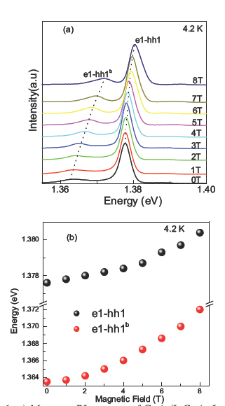
a) Magneto-PL spectra of GaAs/InGaAs Laser
diode structure b) Blue shift of PL peak energy as a
function of B.
It is observed that the luminescence spectrum of
LD structure at low temperature show strong influence
of carrier localization (data not shown here). Fig 6 a & b
show the magneto-PL spectrum of laser diode structure.
The transition energy of localized peak (e -hh b) and 1 1
band to band (e -hh ) peak blue shift with applied 1 1
magnetic field. The shift for localized peak (e -hh b) is 1 1
significantly higher (10 meV) then band to band (e -hh ) 1 1
peak (3 meV). This observation confirms that charge
carrier gets redistributed among the localized states and
give rise to higher energy shift with field. Similarly,
under the extreme perturbation, like high electric field
or current carriers gets redistributed among these states
and therefore may affect the operating wavelength of the
devices and their significance is discussed in the next
section.
D. Emission spectra, L-I characteristics & output
parameters of laser diode arrays:
Initially after processing, all the laser diode
structures are tested under pulsed operation at room
temperature. Lasing action is observed with the range of
threshold current density varied from 100-300A/cm2.
The emission spectrum of laser diode is varied by
changing the material of the active region i.e. the QWs.
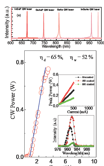
a) Emission spectrum of laser diodes with
different active regions developed at RRCAT b).The CW
L–I characteristics of facet coated single element laser
diode, inset shows the L–I characteristics with and
without facet coating & corresponding emission
spectrum of laser diodes.
Figure 7 a shows the longitudinal spectrum of five
laser diodes operating at different wavelengths. Figure
7b shows the optical output power vs. current (L-I)
characteristics of lasers diodes with and without AR/HR
coatings (inset of the figure). The output power of laser
diodes after facet coatings is also measured from the
front (AR side) and rear facets (HR side) which have the
reflectivity values of 2% and 90% respectively. The
increase in slope efficiency of about 1.82 times confirms
the suitability of ZrO2 facet coating because it is closely
matching with the reported results of the best facet
coated laser diodes with other materials. Inset of Fig. 7b
also shows the emission spectra of laser diode without
and with facets coating. It is noted that the position of
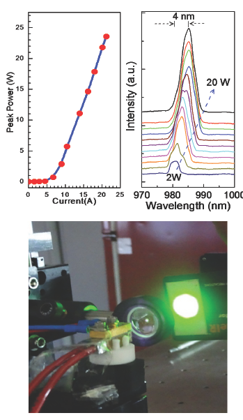
a) L-I characteristics of laser diode arrays &its
emission is shown in the inset photograph b)Emission
spectrum of laser diode arrays at different power level,
c) shows the actual photograph of a 980 nm laser diode
array under operation.
emission spectrum of the facet coated surfaces are
nearly similar to that of uncoated surface. The small
blue shift of ~ 1 nm may be due to the variation of the
operating temperature of the Peltier cooler assembly.
Typically the rate of change of wavelength with
temperature in the semiconductor laser diode is 0.3
nm/K. Subsequently, these lasers, die bonded p-side
down with indium preform on a gold plated copper
package, were also operated under continuous wave
(CW) mode of operation. The total output power from
the facet coated laser diode was ~ 0.75 W at ~3.3A
injection current with the differential quantum
efficiency 65% and the maximum wall plug efficiency ~
52%.
Finally, the laser diode arrays emitting at ~ 980 nm
consists of more than 10 elements are bonded and
packaged on water cooled micro-channel laser
mounting assembly. These laser diode arrays were
successfully operated at 23.5 W peak power with 5.65
ms pulse width at 1 Hz rep rate (Fig. 8 a, b & c). These
laser diode arrays also delivered 3 W output power
under CW mode.
E. Applications of indigenously developed Laser &
Diode Arrays:
One of such bonded and packaged laser diode is
also used as a pump source for exciting PL of InAsP/InP
QW structure to study the electronic transitions. Figure
9 shows the electronic transitions of InAsP/InP QWs
having two different thickness. Similarly, emission light
of the laser diode arrays is coupled to 18 meter long, 400
m diameter, fiber for demonstrating the pumping in a
fiber media (Fig 9b). Fluorescence at around 1080 nm
was clearly recorded at the output of the core region of
18m long fiber (Fig 9c). However, due to absorption
band mismatch between the fiber and emission
spectrum substantial power is leaked out. In order to
reduce this mismatch, we have cooled these laser diode
devices by the circulation of chilled water at ~ 5 C in the
microchannel assembly. A shift of the lasing wavelength
(980 nm) due to junction heating is brought down to < 4
nm while operating them up to 20W peak power under
quasi CW operation.
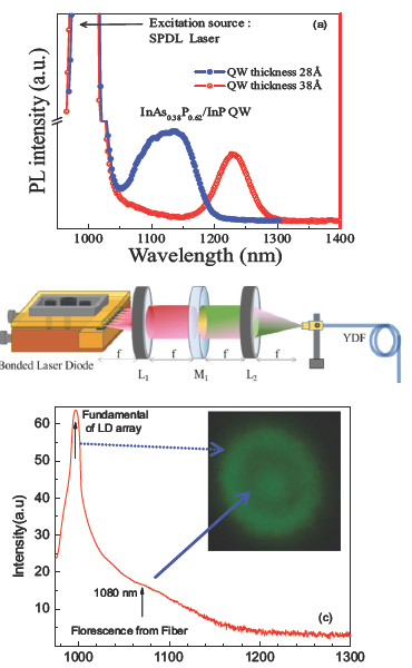
a) PL of InAsP/InP QW structure obtained by
using indigenously developed RRCAT laser b)
Schematic of experimental setup for pumping optical
fiber c) CW emission spectrum and photograph at the
output of 18m long fiber
However the emission wavelength is still higher
than the desired one in order to match with the
absorption band of optical fiber. Thus it is concluded
that device heating alone is not the actual driving force
for the wavelength shifting. Carrier recombination from
the localized states may be responsible for such large
shift and this is also evident from the results of magneto-
PL experiments.
4. Conclusion:
In summary, we have developed high power QW
laser diodes in the wavelength range of 670 to 1000 nm.
Several issues related to epitaxial growth, device
processing, facet coating, bonding & packaging and
testing have been addressed. Significance of the charge
carrier localization on the microscopic parameters are
explained from the temperature, power and magnetic
field dependent photoluminescence. Properties of new
sets of multilayer materials ZrO2 and ZrO2/SiO2 are
investigated for facet coating which assured to have
increased the damage threshold of laser diode arrays.
The processed laser diode emitting at ~ 980nm, is
operated under CW mode with total output power of
0.75 W from the facet coated laser diode with ~ 52%
wall plug efficiency. Subsequently, laser diode arrays
are also developed which delivered 23.5 W peak power
under pulsed operation and 3 W CW power. These
bonded and packaged laser diode can be used for
investigating the material parameters and the same is
proven by using it asa pump source in the
photoluminescence experiments. Further, for high
power application, such as using it as pump source for
fiber laser, significant shift in the emission wavelength
is observed and it is explained due to carrier localization
and heating of the device. The heating of the device is
substantially controlled by the efficient cooling. The
charge carrier localization in the disorder states will be
removed by more controlled growth of the structures.
Successful implementation of these steps will ensure an
efficient coupling of the emission light with fiber for
making fiber lasers.
Acknowledgments:
Authors acknowledge Shri U. K. Ghosh, Shri A. Jaiswal
and Shri G. Jayaprakash for the technical support.
Authors also acknowledge Dr. Aparna Chakrabarti, Dr.
Tapas Ganguli, Dr. B. N. Upadhaya, Dr. Suparna Pal, Dr.
S. D Singh, Dr. R Jangir and Dr. S. M. Oak for their
useful contributions in this work. Authors also
acknowledge Shri P. K. Kush for providing adequate
liquid helium during Magneto-PL experiment. We also
acknowledge colleagues from RRCAT & TIFR for
many useful discussions. Authors also acknowledge Dr.
P. A. Naik, Director RRCAT, & Dr. P. D. Gupta, VC of
HBNI for their constant support during the course of this
work.
|