|
Major Research Areas
R&D on GaN based photodetectors
Recent advances in nitride semiconductors have led to a significant progress in the development of
GaN based optoelectronic devices including light-emitting diodes, lasers and detectors. At RRCAT, our
aim is to fabricate high performance GaN based ultraviolet (UV) photodetectors for potential applications
in high radiation environment. Due to their visible blind nature, radiation-resistance and thermal stability,
these devices offer several advantages over conventional photomultiplier tubes and Si-based UV detectors.
Compared to Si and GaAs-based devices, nitride devices are more radiation tolerant because of a high
displacement energy. It makes GaN a suitable candidate for potential applications in the harsh environments
of nuclear reactors, accelerators and spacecraft. Owing to a wider band gap, GaN based optoelectronic
devices are capable to operate under high electric field often exceeding 1 kV and at high temperatures up
to 600 oC. However, a large density of dislocations of nitride heterostructures is known to be a limiting
factor for both light emitters and detectors. For example, such dislocations play a major role in ‘efficiency
droop’ of near-ultraviolet micro-LEDs fabricated on GaN substrates. Thus, a good control on the dislocation
formation during epitaxial growth and a knowledge of dislocation behaviour are the two pre-requisite for
optimizing the performance of nitride devices. These two issues are suitably addressed where 1) results
from the epitaxial growth of GaN are presented by highlighting the issues related to dislocation density,
and 2) role of dislocations in the performance of GaN based radiation hard UV photodetectors is explored.
An indigenously developed nitride Metal Organic Vapour Phase Epitaxy (MOVPE) system is used for the
epitaxial growth of GaN epitaxial layers. However, the crystalline quality of GaN layers is found to be
rather modest, where a high background carrier concentration makes them unsuitable for photodetector
applications. In-depth electronic transport measurements are thereafter performed on commercially
available MOVPE and Hydride Vapour Phase Epitaxy (HVPE) grown GaN samples. Presence of a highly
conducting interfacial layer is observed in HVPE GaN epilayers. On the other hand, MOVPE GaN epilayers
are found to be free from this limitation which makes them attractive for the device development. Metalsemiconductor-
metal (MSM) PDs are thereafter made on both the samples where the performance of
devices made on HVPE GaN turns out to be better, which is rather surprising. It is explained by citing the
difference in doping method of the GaN epi-layers in the two samples. A method to enhance the detector
performance is demonstrated by the insertion of a thin layer of ZrO2 in metal-oxide-semiconductor (MOS)
geometry. Here, the role of ZrO2 layer thickness is found to be rather critical where the specific detectivity
of PDs is found to be similar or better than the state-of-the-art values reported in literature. Further, a few
devices are also exposed to a high dose of 60Co gamma rays which proves the radiation resistant nature of
indigenously developed PDs along with a fast self-recovery. It signifies the usefulness of the devices for
possible applications in harsh radiation environment. The understanding developed here is expected to be useful for the realization of high performance radiation hard GaN ultraviolet PDs with wide spread photonic
applications.
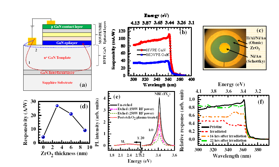
(a) Schematic layer structure of a nitride device grown on top of HVPE GaN templates where the conduction paths
1 and 2 describe the usual and dislocation limited current transport, respectively, (b) Room temperature spectral response
of GaN MSM PDs, (c) Optical microscopic image of the device with oxide inter-layer, (d) Spectral response of GaN PDs
without and with different thickness of ZrO2 layer, (e) Room temperature PL spectra of GaN epilayers before and after
etching with different RF power, (f) Photo response of GaN Schottky photo detector after irradiation with 60Co � source.
Publications from our lab:
- Abhishek Chatterjee, V. K. Agnihotri, R. Kumar, S. Porwal, A. Khakha, Jayaprakash G., Tapas Ganguli and T. K.
Sharma, Sadhana, 45, 249 (2020).
- Abhishek Chatterjee, S. K. Khamari, R. Kumar, V. K. Dixit, S. M. Oak, and T. K. Sharma, Appl. Phys. Lett., 106,
023509 (2015).
- Abhishek Chatterjee, S. K. Khamari, V. K. Dixit, S. M. Oak, and T. K. Sharma, J. Appl. Phys., 118, 175703 (2015).
- Abhishek Chatterjee, S. K. Khamari, R. Kumar, S. Porwal, A. Bose and T. K. Sharma, Superlattices and
Microstructures, 148, 106733 (2020).
- Abhishek Chatterjee, S. K. Khamari, S. Porwal, and T. K. Sharma, Physica Status Solidi: Rapid Research Letters, 3,
1900265 (2019).
- Abhishek Chatterjee, V. K. Agnihotri, S. K. Khamari, S. Porwal, A. Bose, S.C. Joshi and T. K. Sharma, J. Appl. Phys.,
124, 104504 (2018).
- Abhishek Chatterjee, S. K. Khamari, S. Porwal, S. Kher, and T. K. Sharma, J. Appl. Phys. 123, 161585 (2018).
|