|
Major Research Areas
R&D on GaAs based PIN photodetectors for customized applications in DAE
Radiation hard photodetectors are important for various
applications in the harsh environment of high temperature,
high pressure, and high radiation zones. In this context, the
technology for the fabrication of radiation hard GaAs based
p-i-n (PIN) photodetectors has been developed at RRCAT.
The devices work in the wavelength range of 325 to 870 nm
with a maximum responsivity of ~ 0.58 A/W along with a dark
current of < 1 nA and can detect very weak signals of 2 nW
power. Recently, a few customized detector systems are
deployed in field applications, where photodetectors and
necessary front-end electronics are made as per the user
requirements. An early arc detection system as a safety device
is deployed in an indigenously developed radio frequency
circulator at RRCAT. Further, a dual element photodetector
unit, consisting of two identical photodetectors on a chip, is
developed for laser spectroscopy experiments at RRCAT.
Radiation hardness of GaAs photodetectors is tested by
exposing the devices to 60Co g-radiation sources and is found
to be an order of magnitude higher when compared with
commercially available silicon photodetectors.
1. Introduction
Semiconductor photodetectors are an integral part of several
complex systems and find many interesting applications in
the modern life [1-2]. In these devices, the detection of
photons is governed by an effective collection of photogenerated
electron-hole pairs [3-4]. An illumination of a
semiconductor material with photons having energy larger
than the bandgap injects electrons in the conduction band
while leaving a hole in the valence band. Subsequently, the
photo-generated electrons and holes drift in opposite
directions under the influence of either built-in (internal) or
external electric field. Separation of electrons and holes via
this process gives rise to current flow across the device in a
closed-circuit configuration. Here, the magnitude of photo
current depends on the intensity of photon flux, absorption
coefficient of semiconductor material, and quantum
efficiency of the device. In order to have an internal built-in
electric field, several configurations of the structures are
being used. Semiconductor photodetector structures are
designed and developed in many configurations such as
Schottky, p-n and p-i-n (PIN) junction etc. The advantage of
PIN junction configuration is associated with a large depletion width, which results in higher quantum efficiency. A
wide depletion region leads to relatively small capacitance
which results in high bandwidth of detection. Semiconductor
junctions are engineered via an extreme control of dopant
density profile during the epitaxial growth. Out of all the
semiconductor materials, III-V compound semiconductors
have been used to develop key optoelectronic devices for a
variety of conventional and advanced applications over a
wide wavelength range varying from infrared to x-ray region
[3-10]. A few latest breakthroughs have spurred the
development of novel devices by keeping a major focus on the
improvement of peak responsivity, and also the radiation
hardness. GaAs, CdTe, InP, GaN, SiC semiconductor
materials offer higher radiation tolerance against ã-rays,
electrons, protons, and neutrons and can work in harsh
environments over extended durations [7-19] as compared to
Si or Ge. However, in India, fabrication of compound
semiconductor devices is limited to a few R & D labs and a
majority of these devices are being imported even today.
Semiconductor Materials Laboratory at RRCAT have been
working in this area for the last two decades where a major
emphasis is given on R&D of advanced light emitters and
detectors based on conventional group III-V and III-N
compound semiconductors. In this article, salient features of
the fabrication technology of GaAs based PIN photodetectors
are described including the relevant basic physics. Key
parameters asserting the state-of-the-art performance of
indigenously developed devices are also reported.
Representative applications of the devices are highlighted by
providing results from a few experiments. Details of a few
customized detector systems that are fabricated as per the user
requirements are also given. Radiation hardness of these
devices against the exposure to 60Co g-radiation sources is also
discussed.
2. Experimental details
Fabrication procedure of GaAs based PIN photodetectors is
described in this section. It includes epitaxial growth of
multilayer structure, and various devices fabrication steps like
photolithography, metallization, device isolation,
passivation, annealing, wire bonding, packaging, and device
testing.
2.1 Layer structure and growth conditions
The typical layer structure of PIN photodetector consists of an
undoped 5.5 μm thick intrinsic (i-type) layer of GaAs
sandwiched between 20 nm of p-type (~ 2x1018 cm3) and 600
nm of n-type (1x1018 cm3) GaAs layers as shown in Figure
T.4.1(a). Numerically calculated energy band profile of the
photodetector structure is shown in Figure T.4.1(b). In a few
devices, internal gain layers are also embedded in the intrinsic
region of device. GaAs based multilayer structures are epitaxially grown by AIX-200 metal-organic vapor phase
epitaxy (MOVPE) system on 2-inch diameter n+-GaAs
substrates in the temperature range of 600-700 ºC. Tri-methyl
gallium and arsine are used as the precursors while silane and
diethylzinc are used for n and p-type doping respectively.
Each layer of the multilayer stack is individually optimized
with respect to the dopant density, whereas crystalline quality
is optimized by growing an undoped GaAs layer under
different growth conditions. A few calibration growth runs are
therefore needed prior to the epitaxial growth of complete PIN
photodiode structure.
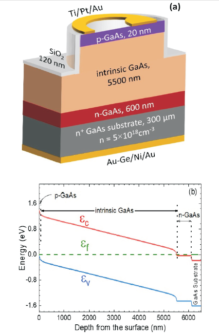
(a) Schematic cross sectional view, and (b) energy
band profile of GaAs p-i-n photodetector
2.2 Device fabrication
After epitaxial growth, fabrication of semiconductor
photodetectors is performed by implementing several device
processing steps. First, Au-Ge/Ni/Au multilayer contacts are
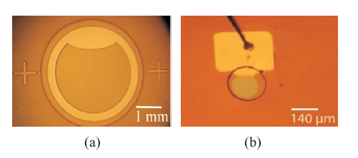
Photographs of GaAs photodetector element
having a diameter of (a) 3 mm, and(b) 100 µm
deposited on the backside of n+-GaAs substrate by thermal
evaporation technique, which is then followed by rapid
thermal annealing (RTA) at 375 ºC for 45 s under nitrogen
environment. Second, the active area of photodetector is
defined through photolithography step. Here, photoresist
(Shipley S1813) is coated on the top of epitaxial structure with
the help of a spin coater. The sample is then exposed to an
ultra-violet beam for a given duration which is then processed
for defining the active area of device. Third, a controlled
chemical etching of epitaxial structure is performed by
dipping the sample in CH3(OH):H3PO4:H2O2(6:3:1) solution
for 10 s at 35 ºC. It helps in defining the active area of device.
Fourth, a layer of SiO with thickness of ~120 nm is deposited 2
on the sample by electron beam evaporation technique [20-
22]. This helps in the passivation of surface states and also in
minimizing the reflection of photons from the detector
surface. Fifth, second photolithography step is performed to
define the top-contact area. Sixth, selective area oxide
removal is carried out by dipping the sample in buffer HF
solution, which therefore provides direct access to p-GaAs
layer in the defined region for the deposition of top-contact as
shown in Figure T.4.1(a). Seventh, Ti/Pt/Au multilayers are
deposited on the designed pattern on the top of the detector
structure, which is then followed by a metal liftoff procedure
and rapid thermal annealing. At the end of seventh step,
fabrication of individual detector element is completed.
Photograph of a large area photodetector element is shown in
Figure T.4.2(a), while that of a 100 mm diameter one is shown
in Figure T.4.2(b). Eight, the detector chip is die attached with
the help of silver epoxy on Au-plated copper mounts, which
provides the back contact. Ninth, 1 mil (~25 m) thick Au wire
is bonded to the front contact by ball-wedge bonding
procedure. It completes the fabrication of photodetector
device which is ready for mounting in specially designed
detector headers as per the requirement of user. Photograph of
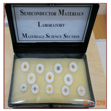
12 numbers of GaAs PIN photodetectors with size varying
from 100µmm to 6 mm diameter is shown in Figure T.4.3.
These detectors are mounted in the indigenously designed device headers. Some of the fabrication steps had to be
customized in order to meet the user requirements that often
vary depending on the complexity of application. One critical
step is to define the size of detector element which is
application specific. For example, for low dark current
applications, a small element size (100 mm or lower) is
preferred. On the other hand, large area photodetectors are
generally preferred by most of the users. In some cases, a very
specialized geometry of detector element is preferred by the
user. One such example from laser spectroscopy is discussed
in the later part of the article. In conventional fabrication
route, one requires a new set of masks for photolithography,
whenever a change in the geometry of detector element is
sought by the user. It is quite inconvenient, since it not only
requires extra funds and time but also discourages newer
developments. Keeping this in mind, a low cost mask-less
photolithography setup is made and is currently being used in
the development of novel semiconductor devices on routine
basis. It is developed by using a digital-projector and a stereozoom
optical microscope [23].
Photograph of 12 numbers of GaAs PIN
photodetectors with element size varying from 100 mm to 6
2.3 Device testing
Operating performance of the devices needs to be checked
through various characterization procedures before their
deployment in field applications. Figure T.4.4 shows the
representative current-voltage characteristics of a
photodetector with 5 mm diameter which can be biased upto
-40 V. For low dark current applications, a specific structure
with internal gain is designed and the performance of such a
device having 3 mm diameter is shown in the inset of Figure
T.4.4 [24]. It is obvious from the inset that the dark current
increases from 5 pA to 2 nA under light exposure. It is also
shown that the device can read laser power down to 2 nW.
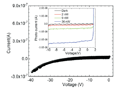
Current-Voltage characteristics of indigenously
developed GaAs photodetector. Inset shows variation in the
reverse saturation photocurrent of a specially designed
device under light exposure at 730 nm.
Next, the responsivity (R) of photodetectors is estimated by
using the relation, R=JA/Pin , where J is photocurrent density, in
A is area of detector element, and Pin is the power of incident in
light. Quantum efficiency (η) and specific detectivity (D*) of
the device are also estimated by using the following
expressions [24-25];
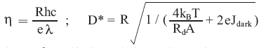
where, h, c, e, λ, and kB have their usual meaning, Rd stands for B d
the dynamic resistance of device, T is temperature in kelvin
and Jdark is the dark current at temperature T. It may be noted dark
that the value of D* might change slightly after including the
generation–recombination process in the active region of the
device. Further, the spectral response of photodetectors is
shown in Figure T.4.5. The detector works in the wavelength
range of 325 to 870 nm with a maximum responsivity of
~ 0.58 A/W at 869 nm and the dark current remains < 1 nA
even for devices having large diameter approaching 10 mm.
The operating characteristics of indigenously developed
photodetectors are summarized in Table T.4.1. These are the
best set of parameters achieved for the indigenously
developed devices, which certifies a state-of-the-art
performance of GaAs PIN photodetectors. It is needless to say
that particular device characteristics can be fine-tuned as per
the user requirement, including the range of spectral response,
which can be tailored by growing a different heterostructure
by MOVPE.
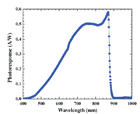
Spectral response of indigenously developed GaAs photodetector.
Operating characteristics of indigenously
developed GaAs photodetectors
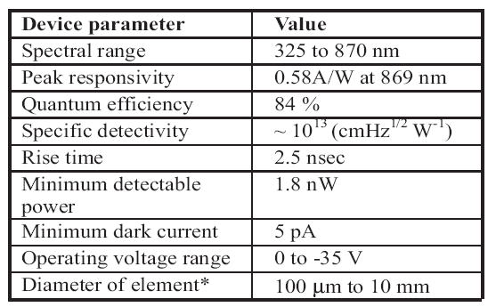
* Diameter of detector element can be varied as per the user
requirement.
3. Deployment of indigenously developed GaAs PIN
photodetectors
Excellent operating characteristics of indigenously
developed devices as shown in Table T.4.1 encouraged us to
look for their possible applications in the departmental work.
A brief summary of the deployment of indigenously
developed GaAs PIN photodetectors is given in this section.
3.1 Application in photoluminescence spectroscopy
Photoluminescence (PL) spectroscopy is a standard method
to characterize the optical quality of epitaxial layers. A strong
PL signal indicates better crystalline quality of the material
under investigation. GaAs PIN photodetectors are used for
measuring the PL spectra of various quantum well (QW)
samples grown in our lab. Figure T.4.6(a) shows the
schematic layer structure of a multi QW structure which is used as a test sample. PL spectrum of this sample is recorded
with the help of a commercially available Si photodetector,
and also with an indigenously developed GaAs photodetector.
The outcome of such an exercise is shown in Figure T.4.6. It
certifies the usefulness of developed devices in PL
spectroscopy.
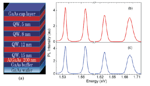
(a) Schematic layer structures of a multi quantum
well structure, and PL spectra of sample recorded with (b)
commercially available Si photodetector, (c) indigenously
developed GaAs photodetector.
3.2 Detection of degree of circular polarization of PL
Spin-photonics is another emerging area where indigenously
developed GaAs photodetectors can play an important role. In
these experiments, detection of the degree of circular
polarization (DCP) of light emitted by QW samples is
correlated with the density of spin-polarized electrons [26]. A
major hurdle in such experiments is to detect a very weak
spin-polarized PL signal, typically of few nW power. In such
an experiment, strength of the signal is mainly governed by
the spin relaxation mechanisms acting in the QW sample. One
usually opts for a photomultiplier tube (PMT) for such
sensitive measurements. Figure T.4.7 shows the outcome of
such an exercise where DCP of a QW sample is measured with
the help of a PMT and also by an indigenously developed
GaAs photodetector.
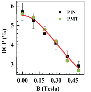
DCP of PL signal of a quantum well sample
measured by using an indigenously developed GaAs
photodetector and a PMT.
It is quite encouraging to see that the indigenous device can
deliver the desired outcome even in such specialized
experiments. From the magnetic field dependence of DCP, an
electron spin relaxation time of 50 ps (± 3.5 ps) is estimated.
This also demonstrates the usefulness of indigenously
developed detectors in the measurement of spin lifetime of
charge carriers in a QW sample.
3.3 Arc fault detection system for RF circulator
Customized single element GaAs based PIN photodetectors
are made for arc fault detection applications in radio
frequency (RF) circulator systems. A quick response of the
sensor is critical for this application. Keeping this in mind, the
temporal response of indigenously developed photodetectors
is measured by using femtosecond laser pulses and is found to
be ~ 2.5 ns. Initially, the performance of GaAs photodetector
for safety operation is checked by developing a lab-based arc
ignition facility. A photograph of this facility is shown in
Figure T.4.8(a). Here, an arc is artificially generated for a predefined
duration and the response of GaAs sensors is tested
with respect to arc test pulse. One representative pulse
recorded by the GaAs sensor is shown in Figure T.4.8(b). It
can be seen that the sensor can read the arc pulse within a
period of < 5 ms, which is sufficient for meeting the user
requirements.
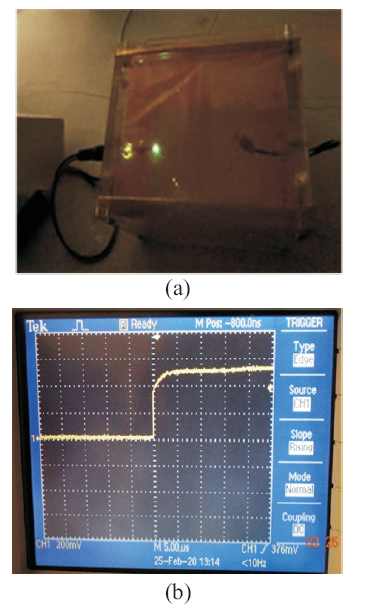
(a) Photograph of a test setup for arc fault
detection. (b) Trace of an arc pulse detected by the GaAs
sensor.
Next, an arc fault detection system is designed and developed
by using a trans-impedance amplifier and GaAs PIN
photodetectors. The system contains mainly three input
channels for the connection of sensors and an LCD display to
show the magnitude of signal corresponding to each sensor. A
schematic diagram of arc fault detection system deployed in a
RF circulator is shown in Figure T.4.9(a). Necessary mounts
for holding GaAs photodetectors are also made as shown in
Figure T.4.9(b). GaAs photodetector elements are placed at
the tip of mount which has a BNC output connector at the
other end. It is ensured that the detector assembly is
compatible with RF environment. Further, the system
contains a scaling circuit and STM-32 microcontroller for the
digitization of analog signals and to display the digitized
signal on a 20x4 LCD screen as shown in Figure T.4.9(c). This
system continuously monitors the three sensors and triggers
an alarm at a pre-settable value. Whenever an arc is detected
by any of the three sensors, it generates an audible as well as
visible alarm.
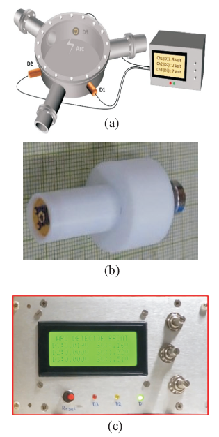
(a) Schematic diagram of arc fault detection system
with three input channels, (b) photograph of an indigenously
developed GaAs sensor for arc fault detection, and (c)
photograph of the control panel of arc fault detection system.
Further, the safety system latches the alarm state until the
same is cleared by the user. Potential free normally-closed
contacts are provided to user as additional safety measure for
shutting down the load in case an alarm is triggered. After a
series of tests in lab, indigenously developed arc fault
detection system is deployed in the RF circulator, developed
by RFSD, RRCAT which primarily works as a safety
interlock for switching off the electrical supply as per the user
requirement. The system is in regular use at RFSD in RF
circulator operating at about 40 kW power.
3.4 Balanced photodetector for laser spectroscopy
applications
Balanced photodetectors find several interesting applications
in laser spectroscopy. Here, one measures the difference in the
intensity of two laser beams, which are of same intensity and a
minor difference is caused by some physical phenomenon. In
order to do this, a very sensitive detection unit is required by
the user that is capable of measuring a very small difference in
the intensity of two laser beams with a high signal-to-noise
ratio. In view of this, balanced photodetectors are quite
attractive since laser noise or any other common noise can be
canceled out. This leads to the detection of a weak signal
overriding on a large DC background. In a balanced
photodetector, two photodetectors are connected in such a
way that the effective output becomes zero, as long as the
intensity of laser beams incident on the two detectors is same.
This imposes a stringent condition to make the performance
of two photodetectors almost identical. In order to achieve
this, two identical GaAs based photodetectors (PD & PD ) are 1 2
fabricated on a single chip as shown in Figure T.4.10(a). The
detectors are of 4 x 7 mm2 size along with a spacing of 3 mm
as required by the user. A rectangular geometry of detector
element is required to accommodate an elliptical laser beam
as per the user requirement. Further, a large size of detectors is
needed to minimize the error due to any minor displacement
of the laser beam during the experiments. In order to minimize
the noise, and also to keep the assembly compact, a special
packaging is designed and developed as shown in Figure
T.4.10(b). The dual detector chip is mounted on a PCB along
with all the readout electronics. The photocurrent from PD1
and PD is amplified by LF356 operational amplifier based 2
trans-impedance amplifiers which is further amplified by
variable gain voltage amplifiers. The amplified signals are
then processed through INA105 precision unity gain
differential amplifier. The dual-element detector along with
the electronics is packaged in a metal box and provision to
read the output of individual detectors along with the
differential signal is made available to the user. The
performance of the complete system is tested by using a
633 nm He-Ne laser. The incident power (P ) on PD is fixed at o
95 ìW and that of PD2 (Po+ÄP) is varied by using a circularly
variable neutral density filter. The dual-element detector is found to be extremely sensitive to the difference in incident
power with a sensitivity of 36 mV/ 1 ìW as shown in Figure
T.4.10(c). It is important to note that such specialized
balanced photodetectors are not commercially available.
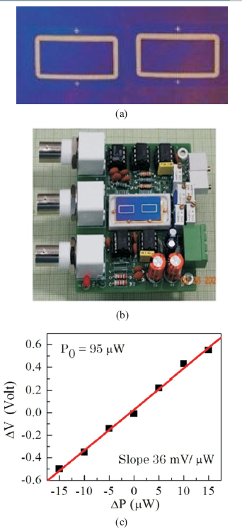
(a) Photograph of dual element GaAs
photodetector chip, (b) Photograph of balanced
photodetector system, where dual element detector is
mounted on top of PCB, (c) the differential signal generated
(ÄV) as a function of difference in incident power (ÄP).
3.5 GaAs based x-ray detectors
GaAs photodetectors find interesting applications in x-ray
region of electromagnetic spectrum due to their radiation
hardness along with a high photon absorption efficiency when
compared to silicon [8-10]. In view of this, prototype x-ray
detectors based on GaAs materials are also fabricated. Such
detectors operating in the range of 20–100 keV are attractive
for medical imaging applications. Silicon detectors are not
ideal for x-ray applications in 20–100 keV range since silicon
has quite a low absorption above 20 keV. In view of this, GaAs
based PIN photodetectors with very thin p-GaAs layer are
specially grown. Photodetectors are fabricated and are
successfully tested against laboratory based CuKa x-ray
source. The energy-dependent x-ray response of GaAs PIN
detector is also measured by using a monochromatic x-ray
beam with energy varying from 8 to 25 keV at BL-2 beamline
of Indus-2 synchrotron radiation source as shown in Figure
T.4.11. It confirms the suitability of indigenously developed
GaAs detectors over a wide x-ray spectral range. Further
refinements for enhancing the signal strength and also to
widen the energy range are in progress.
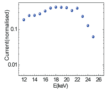
Spectral response of indigenously developed
GaAs based x-ray detector recorded at BL-2 beamline of
Indus-2.
4. Radiation hardness of indigenously developed GaAs
based PIN photodetectors
GaAs is expected to be radiation hard when compared with
commercially available silicon photodetectors. In view of
this, GaAs photodetectors were exposed to 360 kGy of ãradiation
[23-25]. All the irradiations were performed at room
temperature in a 2490 Curie 60Co gamma chamber (Model No;
GC-900) supplied by the Board of Radiation and Isotope Technology, Mumbai. After the exposure of GaAs detectors to
ã-rays, an increase in the dark current per unit volume (J ) is v
seen as a function of ã-ray fluence (F) as shown in Figure
T.4.12.The slope (á = DJv/DF) of the current per unit volume
versus ã-ray fluence is estimated to be ~5 x10-l9 A/cm for GaAs
which is lower by an order of magnitude when compared to Si.
A lower value of á confirms that radiation tolerance of GaAs
is more than that of Si, particularly in the high flux ã-ray
environment. Results shown in the inset of Figure T.4.12
confirm that there is a significant recovery of the radiation
damage as the time elapsed after the irradiation. Such an
improvement is predominantly due to the reduction of carriers
contributing to the saturation current. Thus, it is proven that
the radiation induced defects can be partially recovered even
without any high temperature annealing step [27-29]. Such a
self-recovery of GaAs based devices is really attractive. Due
to such attributes, GaAs based detectors are attractive for
many applications in high temperature, high radiation zones,
for example direct electron detection spectrometer, and also
for space science missions [30-32].
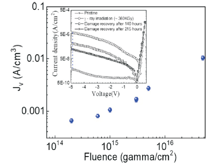
Reverse saturation current per unit volume as a
function of irradiated dose, inset shows the recovery of
radiation induced damage as a function of cumulated
annealing time at RT.
5. Conclusion
A complete technology for the fabrication of GaAs based
photodetectors is developed. It involves design and multilayer
growth by MOVPE technique and various devices fabrication
steps that are needed for the fabrication of GaAs detector
chips. The fabrication steps are also optimized for customized
applications. Thereafter, GaAs based photodetectors are used
in spectroscopy experiments to record the PL spectra of
various QW samples. Performance of GaAs based detectors is
found to be similar to that of commercially available silicon
photodetectors. GaAs based photodetectors are found suitable to replace the PMT in low noise applications for
measuring the DCP of PL signal emitted by a QW sample. An
arc fault detection system based on GaAs photodetectors is
also developed and is deployed in RF circulator as a safety
system to switch off the load in case an arc is detected. A
balance photodetector assembly is developed by
incorporating a custom built dual detector chip for interesting
applications in laser spectroscopy. GaAs based x-ray
prototype detectors are also made which works in the energy
range of 12 to 25 keV. It demonstrates our capabilities for the
development of customized radiation hard photodetectors
based on GaAs epitaxial layers. Development of a few more
customized semiconductor photodetectors as per the needs of
RRCAT users is in progress. Finally, the radiation tolerance of
GaAs photodetectors is measured by exposing the devices to
360 kGy of ã-radiation. The devices were found to be
operational even after exposure to such a high dose and their
radiation tolerance is found to be an order of magnitude higher
when compared with commercially available silicon photo
detectors. The technology developed here can find several
interesting applications in the harsh environment of high
temperature, high pressure, and high radiation zones.
Acknowledgement
In this article, we have summarized the work which has been
carried out by the entire team of Semiconductor Materials
Laboratory during the last few years and their contribution is
hereby acknowledged. We acknowledge the colleagues from
RFSD, LPAS, SUS, FSOSS, LCID, Laser Workshop and
Chemical Treatment Laboratory, who had made useful
contributions. In particular, Dr. Ashish Kumar Tiwari, RFSD,
Dr. S. P. Ram, LPAS, and Dr. S. K. Rai, SUS contributed in the
development of customized devices. Authors would like to
thank Shri S. V. Nakhe, Director, Materials Science Group
and Shri Debashis Das, Director, RRCAT for their constant
support and encouragement.
|