Photonics nanomaterials
We are engaged in R&D on the growth and characterization of nanostructured materials and their application related studies for the development of photonic devices and components such a photovoltaic cells, solar light based water splitting for hydrogen generation, solar-thermal heating, OFET based gas/chemical sensor etc. Brief account of activity details on material development, device fabrication and characterization tools are as follows.
- Synthesis of Organometallic halide perovskites (OMPs) precursors for photovoltaic device applications
Lead halide based Organometallic perovskites (MAPbX3: MA = CH3NH3+ , X = I-, Br- or Cl- ) have gained interest due to their tunable optical band gaps, desirable electronic properties and low cost deposition techniques. We are exploring the solution based thin film deposition methods which are often based on spin coating of the precursors. In this regard two deposition methods namely one-step direct deposition as well as two-step (sequential deposition) methods have been carried out at ambient as well as in inert atmosphere glove box system. Laser irradiation based annealing studies are also being carried out to improve the crystalline quality of these materials.
- Lead bromide based single crystal perovskites
Highly luminescent single crystals of MAPbBr3 were synthesized using equimolar ratio of precursor materials MAPbBr and PbBr2 in DMF under stirring at a constant temperature at ~800 °C overnight without using any additives. The characterization of these crystals have been done using XRD, PL and UV-Visible absorption/PL spectroscopy. Detailed studies on charge carrier trapping using thermally stimulated current were carried out.
- Studies on Au-TiO2 nanocomposites
TiO2 is used extensively as UV light induced photoactive materials in photocatalytic and photoelectrochemical device applications. To make these materials responsive to visible solar light, it is desirable that material absorbs over visible spectral range. With that aim we fabricated Au-TiO2 nanocomposites using laser ablation in liquid phase method. Here nanosecond laser based ablation of Ti metal dipped in water generate TiO2 nanoparticles. We also added HAuCl4 salt dissolved in water so as to simultaneously generate Au nanoparticles in the ablation plasma plume. Detailed characterization studies showed formation of nanocomposite of Au nanoparticles anchored onto TiO2 nanoparticles. With increasing Au content on to TiO2 provided shift of TiO2 absorption band gap from UV to visible range. Detailed characterization studies suggested charges redistribution at the interface of two nanoparticles together with the surface plasmon induced field enhancement are possible reasons of red shift in the absorption band gap of TiO2.
- Thermoplasmonic materials for solar-thermal heating
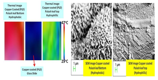
We fabrication and characterized bio-inspired hierarchical metallic nanostructures as an efficient absorber of broadband solar light radiation for solar-thermal conversion applications. We used pulsed laser deposition to deposit different thicknesses of Cu nanostructures on the bottom (hydrophobic) and top (hydrophilic) surface of Palash leaf (scientific name “Butea Monsperma”). Optical image and reflectivity data of two surfaces coated with Cu showed clear advantage of coating metal on hydrophobic side of leaf for efficient absorption and temperature increment upon solar irradiation. The naturally occurring hierarchical bio-structures on the bottom hydrophobic surface of these leaves are responsible for similar hierarchical micro/nano structures of Copper. These hierarchical Cu nanostructures with wide range of size and shape enables excitation of surface plasmons over a broad range of optical spectrum and black color appearance of Cu coated leaf. Thermal images of these surfaces under white light showed substantial rise of surface temperature (Figure 1) in comparison to planar Cu film of similar thickness deposited on a glass plate. Maximum temperature rise and the rate of temperature rise has been correlated with absorption strength and local field enhancement by invoking a simple model based on surface plasmon resonance.
|
Figure 1. (a) The thermal image of Copper coated on two sides of Palash leaf and also bare Cu film of glass slide. (b) SEM image of Copper coated on bottom shows abundant nanograss like structure and top surface of Palash leaf does not show any nanograss like structure. |
- Development of Thermally Stimulated Current measurement setup
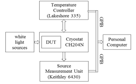
Thermally stimulated current (TSC) measurement is a widely employed method to probe electronic trap states of charge carriers generated using suitable light sources. TSC spectra, current vs temperature plot, provides trap energy distribution present in the material. TSC set up consist of a cryostat, temperature controller, source-measure unit (SMU) and light source. For collecting the TSC data of device under test (DUT), every instruments needed to be synchronized. The output of the temperature controller and SMU are to be read accurately during the temperature ramp, which asserted the need of automation. Details of the measurement setup is shown in Figure 2. LabView based automation software was used for desired synchronization, data handling, monitoring and controlling of the instruments during experiment. To confirm the reliability of the developed set up, TSC spectra of Poly[2-methoxy-5-(3’,7’-dimethyloctyloxy)-1,4-phenyle (MDMO-PPV) polymer and methyl ammonium lead iodide (MAPI) perovskite was reproduced.
|
Figure.2 TSC setup and front panel display of automated data acquisition. |
- Fabrication of Polymer and perovskite based photovoltaic devices
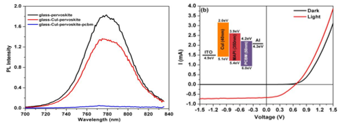
We use inert atmosphere glove box system for fabricating photovoltaic devices. It is equipped with hot plate, spin coater, thermal evaporator, fiber coupled solar simulator, device test fixture and I-V measurement system. We fabricated perovskite based PV cell with device structure of ITO/CuI/ Methyl Ammonium Lead iodide (MAPI, Perovskite layer)/phenyl-C61-butyric acid methyl ester (PCBM)/Aluminum (Al) and obtained cell parameters as Voc= 0.65V, Isc=0.67mA, Fill Factor = 0.41 and PCE=~4%, under standard AM1.5 one sun illumination (Figure 3). Since efficiency being low so it demanded optimization of fabrication process with desired material properties. Effort is on to adopt suitable processing conditions to obtain highly crystalline and stable perovskite thin films.
|
Figure 3 (a)Photoluminescence quenching of MAPI with different active layers. (b) I-V characteristics of fabricated PSC. (Voc= 0.65V, Isc=0.67mA, fill factor =0.41 and PCE=4%.). Inset shows energy level diagram of PSC. |
- Development of characterization tools
- Transient photo-conductivity
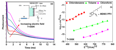
Time-of-Flight (TOF) based Transient photo-conductivity measurement set up is developed to measure drift mobility and to investigate nature of charge transport in thin films of photovoltaic materials. Studies on pristine and doped thin films of Poly(2-methoxy-5-(3′,7′-dimethyloctyloxy)-1,4-phenylenevinylene) (MDMO PPV) showed strong role of casting solvent and nanomaterial dopants in governing the polymer film morphology and charge transport. Figure 4(a) inset shows schematic of TOF measurement.
|
Figure 4 (a)Typical TOF photocurrent pulses with applied electric field (b) Field dependence of mobility in MDMO PPV thin films casted using different solvents. |
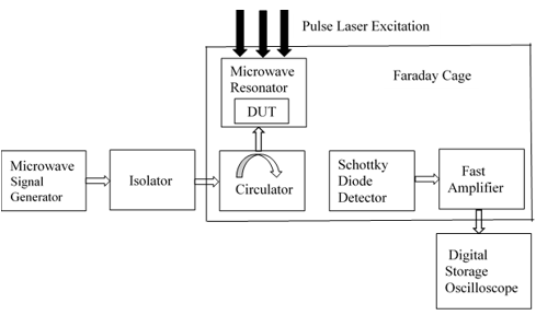
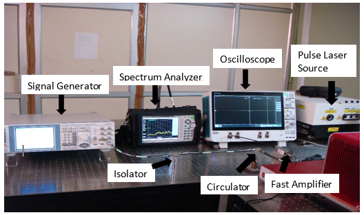
- Development of Flash-Photolysis Time Resolved Microwave Conductivity Experimental Setup
Flash-photolysis time-resolved microwave conductivity (TRMC) monitors dynamics of photo-excited charge carriers on the ns-μs timescale, making it an ideal tool for investigating charge carrier recombination processes or intrinsic carrier mobility of material at bulk and nanoscale. This is contactless technique that help avoid complications arising from contact electrodes such as recombination at the electrode/material interface, back injection of charges etc. Due to the versatility of this technique, TRMC has been applied to study wide range of materials in the form of solution, solid or gas-phase. With these objectives the development of TRMC measurement set up is being carried out. Here X-band MW (8-12 GHz) is used as probe is measure changes in conductivity of a given material upon pulsed photoexcitation. Assembly of sub components of the system such as Gunn Diode, Isolator, Circulator and detector etc. is shown in Figure 5. Microwave resonant cavity with provision of laser excitation was fabricated and initial reflectivity measurements of conjugated polymer MDMO-PPV were carried out.
|
|
Figure 5. Schematic block diagram and experimental set up of TRMC |
Equipment and resources:
- Wet chemistry lab equipped with fume hood, vacuum oven, hot plate and spin coater, ultrasonic bath cleaner etc.
- Integrated glove box system with thermal evaporation system for device fabrication in inert environment
- Steady state and time resolved photoluminescence measurement (UV-VIS-NIR) system (decay time from ~200 ps to microsec, RT temp to 10K and emission range 300nm to 1600nm)
- Transient and steady state photoconductivity measurement system
- High voltage poling setup for developing poled polymers for NLO applications
- Surface profiler for thickness and roughness measurement
- Wavelength tuneable 10 Hz, 5 ns pulsed OPO laser (tuneable range ~ 410-1800nm)
- Thermal evaporation system
- Impedance measurement system
- Contact angle measurement system
- Solar simulator
- Plasma cleaner system for surface cleaning
- Source measurement unit for I-V and C-V characterisation of devices
- Liquid and vacuum phase pulse laser deposition setup with Q-switched Nd:YAG laser as source.
Additional resources under development
- Femtosecond laser based generation and creation of micro/nano structures for Photonics Applications
- Thermally stimulated luminescence measurement setup
Team members:
- Dr. M. P. Joshi, SOH, (Head)
- Dr. T. S. Dhami, SOG
- Dr. Uday Chakravarty, SOF
- Sh. Jai Khare, SOF
- Dr. S. Raj Mohan, SOF
- Dr. R. S. Verma, SOF
- Smt. A. Chaturvedi, SOE
- Sh. Vikas Jain, SOD
- Sh. Nitin Madokar, Tech/D
Recent peer reviewed journal publications (during 2016-2021)
- 'Influence of Alkyl Chain Length on Mobility of P3ATs studied by Photoinduced Extraction Current Transient Technique',
K. Bhargava, A. Bilgaiyan, S. Raj Mohan, M. O. Ittoop, M. P. Joshi, L. M. Kukreja, V. Singh,
J.Nano. Sci. and Nano Tech. , 16, 3241, 2016.
- “Dimensional crossover of electron weak localization in ZnO/TiOx stacked layers grown by atomic layer deposition"
Saha, D., Misra, P., Bhartiya, S., Gupta, M., Joshi, M.P., Kukreja, L.M.,
Appl. Phys. Lett.108(2016) 42109.
- “Observation of dopant-profile independent electron transport in sub-monolayer TiOx stacked ZnO thin films grown by atomic layer deposition”
Saha, D., Misra, P., Das, G., Joshi, M.P., Kukreja, L.M.,
Appl. Phys. Lett. 108(2016)32101.
- “Corroboration of Raman and AFM mapping to study Si nanocrystals embedded in SiO2”
Ekta Rani, Alka A. Ingale, A. Chaturvedi, M. P. Joshi and L. M. Kukreja,
J. of Alloys and Compounds, 672, 403 (2016).
- “Growth of Anatase and Rutile Phase TiO2 Nanoparticles using Pulsed Laser Ablation in Liquid: Influence of Surfactant Addition and Ablation Time Variation”
Amita Chaturvedi, M. P. Joshi, P. Mondal, A.K. Sinha, A. K. Srivastava,
Appl. Surf. Sci. 396 (2017) 303-309.
- “Band gap tuning in Si-SiO2 nanocomposite: Interplay of confinement effect and surface/interface bonding”
Ekta Rani, Alka Ingale, D. M. Phase, A. Chaturvedi, C. Mukherjee, M. P. Joshi and L. M. Kukreja,
Appl. Surf. Sci., 425, 403 (2017).
- “Comment on “Structural and Electrical Properties of Atomic Layer Deposited Al-Doped ZnO Films”.
Saha, D., Misra, P., Joshi, M. and Kukreja, L. M.,
Adv. Funct. Mater., 1702875 (2017).
- “ Correlation of size and oxygen bonding at the interface of Si nanocrystal in Si-SiO2 nanocomposite: A Raman mapping study”,
Rani, E, Ingale, A, Chaturvedi, A, Kamal, C, Phase, DM, Joshi, MP, Chakrabarti, A, Banerjee,, Kukreja, LM,
J. Raman Spec., 47, 457 (2016).
- “UV light induced insulator-metal transition in ultra-thin”, ZnO/TiOx stacked layer grown by atomic layer deposition”,
D. Saha, P. Misra, M. P. Joshi, and L. M. Kukreja,
J Appl. Phys. 120( 2016) 085704
- “Charge transport in thin films of MDMO PPV dispersed with lead sulfide nanoparticles",
S Raj Mohan, M. P. Joshi, T. S. Dhami, V. Awasthi, C. Shalu, B. Singh, V. Singh,
Synthetic Metals, 224 (2017) 80.
- “Influence of Film Morphology on Transient Photocurrent Pulse Shape in Organic Thin Films: A Monte Carlo Study”,
S. Raj Mohan, Manoranjan P. Singh, M. P. Joshi,
Journal of Self-Assembly and Molecular Electronics, Vol. 1, 1–16 (2017).
- “Structural and optoelectronic characterization of organic vapor phase deposited thin films of oriented DH6T molecules”,
Shalu C., S. Raj Mohan, M. P. Joshi, and V. Singh,
AIP Conference Proceedings 1832, 080056 (2017).
- “Investigating Optical Properties of Atomic Layer Deposited ZnO/TiOx Multi-stacked Thin Films Above Mott Critical Density”,
Saha, Debabrata; Misra, P.; Joshi, M. P.
; et al. , J. Phys. Chem. C 121,18129-18136 (2017).
- “Solvent assisted improvement of the dielectric properties and hysteresis behavior in poly-4-vinylphenol(PVP) thin flms”,
Shalu C., Mukesh P. Joshi, Vipul Singh,
Microelect. Eng. 198, 85–92(2018).
- “Charge transport in thin films of MDMO PPV dispersed with lead sulfide nanoparticles”,
S Raj Mohan, M. P. Joshi, T. S. Dhami, V. Awasthi, C. Shalu, B. Singh, V. Singh,
Synthetic Metals, 224 (2017) 80.
- “Influence of Film Morphology on Transient Photocurrent Pulse Shape in Organic Thin Films: A Monte Carlo Study”,
S. Raj Mohan, Manoranjan P. Singh, M. P. Joshi,
Journal of Self-Assembly and Molecular Electronics, Vol. 1, 1–16 (2017).
- “All Organic near Ultraviolet Photodetectors based on Bulk Hetero-Junction of P3HT and DH6T”,
Shalu C., Nidhi Yadav, Kshitij Bhargava, Mukesh P. Joshi, Vipul Singh,
Semicond. Sci. Technol. 33, 095021 (2018).
- “A Model for Charge Transport in Semicrystalline Polymer Thin Films”,
S. Raj Mohan, Manoranjan P. Singh, M. P. Joshi,
J. Polym. Sci. B: Polym. Phys. 57, 137-141 (2019)
- “Effect of concentration of DH6T on the performance of photoconductor fabricated using blends of P3HT and DH6T”,
Shalu C. , Kshitij Bhargava, Nidhi Yadav, Mukesh P. Joshi, Vipul Singh,
Opt. Mater, 89, 214-223 (2019).
- “Monte Carlo simulation of charge transport in disordered organic systems using buffer lattice at the boundary”,
S. Raj Mohan, Manoranjan P. Singh, M. P. Joshi,
Pramana-Journal of Physics, 93:8 (2019).
- "Development of Soft X-ray Excited Optical Luminescence (XEOL) Measurement Setup at Beamline 4 in Indus-1 Synchrotron Radiation Source",
Ravi S. Verma, Praveen K. Yadav, Mukesh P. Joshi,
AIP Conference Proceedings 2265, 030215 (2020).
- “Influence of precursor solution temperature on the crystalline nature of mixed halide perovskite thin films grown by one-step deposition method”,
S. Raj Mohan, M. P. Joshi, T. S. Dhami, S. K. Rai, R. Singh,
Journal of Materials Science: Materials in Electronics volume 32, pages2459–2470(2021).
- “A simple numerical and analytical analysis of Covid-19 progression, infection inhibition and control in various countries”,
U Chakravarty, D Chaturvedi, M.P. Joshi,
Disaster Advances, 14 (3) March (2021).
|