The energy storage nano-capacitors based on ultra-thin multi-stacks of TiO2/Al2O3, TiO2/MgO and ultrathin films of Lanthanides are being grown using atomic layer deposition and pulsed laser deposition techniques and their electrical properties are being studied in metal-insulator-metal capacitor configuration for high density energy storage applications. Interface controlled Maxwell–Wagner relaxation resulting in giant dielectric constant will be realized in these multi-layered stacks by tuning interlayer thicknesses which is highly desired for nano capacitors based energy storage applications.
Doped ZnO thin films for transparent electronics
1. Quantum corrections to conductivity in Si doped ZnO thin films
We have grown Si doped ZnO thin films with Si concentration in the range from 0.5 to 5.8% using sequential pulsed laser deposition. The lowest resistivity obtained was ~ 4.6×10⁻⁴ Ω-cm at a Si concentration of ~ 1.7%. Although the electron concentration in the films were higher than the Mott critical density, the temperature dependent resistivity measurements in the range from 300 to 4.2 K revealed negative TCR for the 0.5, 3.8 and 5.8% Si doped ZnO films in the entire measurement temperature range. The 1.0, 1.7 and 2.0% Si doped films showed a transition from negative to positive TCR with increasing temperature. The temperature independent nature of electron concentration together with the negative low field magnetoresistance found in the films at low temperatures pointed to weak localization as the dominant contributor towards negative TCR. A phenomenological fit of the temperature dependent resistivity data for all the films could be obtained by considering the quantum corrections to conductivity arising due to disorder induced weak localization effect, wherein both the influences of electron-electron and electron-phonon inelastic dephasing processes were included using Matthiessen’s rule. 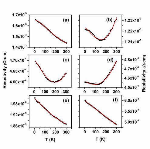
Temperature dependent resistivity (filled circles) of the Si doped ZnO films with Si doping concentrations of (a) 0.5, (b) 1.0, (c) 1.7, (d) 2.0, (e) 3.8, and (f) > 5.8 %.
2. Phase-coherent electron transport in (Zn, Al)Ox thin films
A clear signature of disorder induced quantum-interference phenomena leading to phase-coherent electron transport was observed in (Zn, Al)Ox thin films grown by atomic layer deposition (ALD). The degree of static-disorder was tuned by varying the Al concentration through periodic incorporation of Al2O3 sub-monolayer in ZnO during ALD. It was observed that instead of periodic incorporation of insulating Al2O3 sub-monolayer into the conducting ZnO matrix, the electron transport in these films was effectively three-dimensional. All the films showed small negative magnetoresistance (MR) in the entire range of the measurement temperature (5-200K) and magnetic field (0-8T) due to magnetic field suppressed weak-localization effect as shown in a particular case of (Zn, Al)Ox with Al ~ 3.8 at.% in the following Figure. The temperature dependence of phase-coherence length ( ) extracted from the magnetoresistance measurements (refer following Figure), indicated electron-electron scattering as the dominant dephasing mechanism. The persistence of quantum interference at relatively higher temperatures up to 200 K is promising for the realization of phase-coherent electron transport devices. ) extracted from the magnetoresistance measurements (refer following Figure), indicated electron-electron scattering as the dominant dephasing mechanism. The persistence of quantum interference at relatively higher temperatures up to 200 K is promising for the realization of phase-coherent electron transport devices.
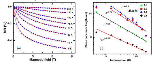
Figure 4 (a) Magnetic field dependent (0-8 T) MR of all the (Zn, Al)Ox thin films with 3.8 at.% Al at different temperatures in the range of 5-200K. The solid lines show the fitting of the experimental data (b) Variation of phase coherence length with temperature for all the (Zn, Al)Ox thin films with Al ~ 1.4, 1.9, 3.2, and 4.7 at.%
3. Dimensional crossover of weak localization in (Zn, Ti)Ox thin films grown by ALD
We have investigated temperature dependent electron transport in a series of (Zn, Ti)Ox thin films with well-defined and spatially-localized dopant distribution along the vertical direction of the host ZnO lattice. These films were grown by atomic layer deposition through in-situ incorporation of sub-monolayer TiOx and subsequent overgrowth of conducting ZnO spacer layer. Film thickness was varied in the range of ~ 6-65 nm by varying the number (n= 1 to 7) of vertically stacked TiOx sub-monolayers with nearly identical dopant-profiles. The evolution of sheet resistance versus temperature with decreasing film thickness showed a metal to insulator transition (MIT). On the metallic side of MIT, magnetotransport data were analyzed within the framework of electron weak localization in the diffusive transport regime. Moreover, we found strong evidence for a smooth crossover from two-dimensional to three-dimensional weak localization effect in the temperature dependence of both the zero-field sheet resistance and inelastic scattering length. The results of this study have potential impact on the emerging field of nano-scale transparent oxide-electronics.
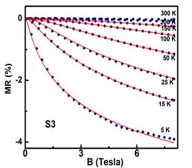 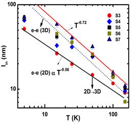
Magnetoresistance data in varying magnetic field (0-8 T) for the sample S3 at different temperatures in the range of 5-300K. The solid lines show the fitting of the experimental data according to 2D WL regime and 3D WL regime. Inset shows variation of inelastic scattering length ( ) with temperature (T). The solid lines are least square fittings of ) with temperature (T). The solid lines are least square fittings of  versus T plots for the samples S3 and S7. versus T plots for the samples S3 and S7.
References:
- A. K. Das et al., Electron interference effects and strong localization in Cu doped ZnO thin films, Materials Science in Semiconductor Processing 68, 2017, 275-278.
- R. S. Ajimsha et al., Observation of weak localization and phase coherent electron transport in sparsely doped (Zn: Ga) O thin films, Journal of Alloys and Compounds 708, 2017, 73-78.
- D. Saha et al., UV light induced insulator-metal transition in ultra-thin ZnO/TiOx stacked layer grown by atomic layer deposition, J. Appl. Phys. 120(8), 2016, 085704.
- D. Saha et al., Dimensional crossover of electron weak localization in ZnO/TiOx stacked layers grown by atomic layer deposition, Appl. Phys. Lett., 108(4), 2016, 042109.
- D. Saha et al., Observation of dopant-Profile independent electron transport in sub-monolayer TiOx stacked ZnO thin films grown by atomic layer deposition, Appl. Phys. Lett. 108(3), 2016, 032101.
- A. K. Das et al., Effects of electron interference on temperature dependent transport properties of two dimensional electron gas at MgZnO/ZnO interfaces, Appl. Phys. Lett. 107(10), 2015, 102104.
- R. S. Ajimsha et al., Observation of low resistivity and high mobility in Ga doped ZnO thin films grown by buffer assisted pulsed laser deposition, J. Alloy Comp.638, 2015, 55-58.
- S. D. Shinde et al., Role of Al doping on micro/structural, electrical, optical characteristics of as deposited and annealed ZnO thin films, RSC Advances 5(31), 2015, 24178-24187.
- D. Saha et al., Phase-coherent electron transport in (Zn, Al)Ox thin films grown by atomic layer deposition, Appl. Phys. Lett. 105(21), 2014, 212102.
- D. Saha et al., Effect of disorder on carrier transport in ZnO thin films grown by atomic layer deposition at different temperatures, J. Appl. Phys. 114(4), 2013, 043703.
- A. K. Das et al., Studies on temperature dependent semiconductor to metal transition in ZnO thin films sparsely doped with Al, J. .Appl. Phys., 112, 2012, 103706.
- R. S. Ajimsha et al., Electrical and optical properties of Dy doped ZnO thin films grown by buffer assisted pulsed laser deposition, Physica E 42, 2010, 1838-1843.
- A. K. Das et al., Effect of Si doping on electrical and optical properties of ZnO thin films grown by Sequential Pulsed Laser Deposition, Journal of Physics D: Applied Physics 42, 2009, 165405.
|