|
|
| Laser Materials Processing Division |
Oxide nano-electronics
Resistive switching in metal oxide nanostructures for non-volatile memory applications |
Resistive memory switching in ultra-thin films of metal oxides have recently shown tremendous potential to overcome the physical and technological limitations of existing CMOS based flash memory technology. The resistive switching (RS) memory devices store information through transition between two states of resistances (low and high) on application of bias voltage in contrast to flash memory which is based on charge-storage. The unipolar resistive switching in metal oxide films has been instead attributed to the formation and dissolution of nano sized conductive filaments (CF) across the oxide layer which mainly comprises of oxygen vacancies and metallic ions. The size and number of such CFs can be varied by varying compliance current during switching events. However, some of the prevailing issues in resistive switching memories include lack of information on RS time, i.e. how fast is switching process from one state to other state, and capability of multiple bit storage in same memory element. We have addressed these issues and observed that multiple nonvolatile resistance states with reasonably good resistance contrast can be obtained in metal oxide thin film based resistive switching memories by precisely controlling the compliance current during switching events. Further we have studied the dynamic evolution of resistive switching events to measure the set and reset switching (write and erase) times and found that set switching process is ~ 104 times faster than reset switching process. For all these studies the metal oxide thin films of desired thickness and chemical compositions were grown by using optimized PLD process or ALD process. The top electrodes were deposited by DC sputtering using shadow mask. Results of our studies in these areas are presented below:
|
| |
Multilevel resistance switching in SmGdO3 thin film |
We observed multilevel resistance switching in amorphous ternary rare earth oxide SmGdO3 (SGO) thin films grown by PLD. In comparison to polycrystalline materials, which contain grains and downscaling of memory cell is limited by the grain size, amorphous materials free from grain and grain boundaries are capable of offering homogeneous structure to avoid scaling issue. The amorphous SGO thin films of the thickness of ~ 50 nm have been deposited by pulsed laser deposition method on the commercially available Pt/TiO2/SiO2/Si substrates at the fixed temperature of 300 °C and in oxygen ambient at a partial pressure of ~ 30 mTorr. The KrF excimer laser operating at a fluence of ~ 1.8 J/cm2 was used for the ablation of the ceramic SGO target. To fabricate metal-insulator-metal (MIM) capacitor structures the Pt top electrodes of thickness ~ 50 nm and the diameter of ~ 80μm were deposited at room temperature by dc-magnetron sputtering using shadow masking. The switching characteristics and conduction mechanisms of these devices were studied through current-voltage (I-V) measurements in the top-bottom configuration. Reliable and repeatable resistance switching with good endurance and retention characteristics was observed in Au/SGO/Pt devices using DC sweep measurements.
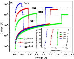 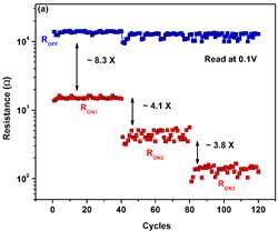
(Left) The I-V curves of the device with different compliance currents (ICC = 1, 3, and 5mA). Inset shows the statistical distributions of different resistance levels, (Right) The endurance of the Pt/SGO/Pt ReRAM device over 120 cycles with different ICC.
To achieve multilevel resistance switching i.e., different resistances corresponding to low resistance state (LRS), the compliance currents was varied during the set process, as shown in figure in left. It was observed that the higher the ICC imposed on the device, the lower resistance value was obtained in LRS. Under different ICC values of 1, 3 and 5mA, the four switching states with different resistance values could be clearly distinguished and the statistical distributions of these four states are depicted in the inset of this figure. The endurance of the device under different compliance current has been performed up to 40 cycles, as shown in figure in right. The resistances were measured at 0.1 volt. The resistances of LRS (ON-sate) are labelled as RON1, RON2, and RON3, under the ICC of 1, 3, and 5mA, respectively. The resistance of the HRS is denoted as ROFF, which has been observed almost same for different applied ICC. According to this figure (right), a considerable resistance window between different resistance states was observed after set/reset cycling stress tests, which is sufficient for the purpose of practical device application. Moreover, the retention characteristics of these four different resistances indicated that each memory state was preserved stably without degradation over 104 seconds. |
| |
Measurement of resistive switching times in NiO film |
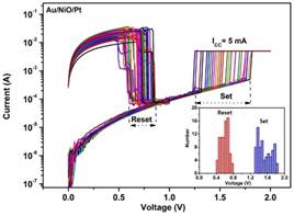
One of the important concerns in unipolar resistive memory switching in metal oxide thin films is lack of information on RS time and its dependence on other switching parameters. We have investigated the dynamic processes during RS of NiO thin film to evaluate RS time and its dependence on compliance current. For these studies ~ 20 nm thick polycrystalline NiO films were grown on commercial Pt/TiO2/SiO2/Si substrates using optimized pulsed laser deposition. Top electrodes of ~ 50 nm thick Au film with a typical diameter of ~ 200 μm were used to construct Au/NiO/Pt metal-insulator-metal structures. Nonvolatile unipolar RS was repeatedly observed in these devices through current-voltage measurements in top-bottom configuration on application of suitable electrical bias. To measure the switching time of RS events namely set (switching from high to low resistance state) and reset (switching from low to high resistance state) processes, the required voltage pulse with predetermined pulse width was applied using Keithley source meter and a digital storage oscilloscope (400 MHz, LeCroy make) was used to record both the voltage pulse applied across the device and current flowing through device simultaneously. The resistive switching in DC sweep is shown in figure in right where in clear switching with well-defined set and reset voltage window has been observed. The dynamic evolution of set switching event is shown in figure in right. From the enlarged view as shown in inset of this figure, the set switching time have been evaluated to be ~ 10ns for compliance current of ~ 5mA. Repeatedly the set process was found to be varying statistically in the range of ~ 8 – 30 ns and unaffected by compliance current.
 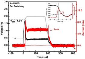
(left) Typical DC resistive switching characteristics of NiO thin film in Au/NiO/Pt structure. Inset shows the distribution of set and reset voltages. (right) Dynamic evolution of set switching processes where applied voltage pulse across the Au/NiO/Pt device and measured current pulse are shown. Inset in figure shows zoomed current and voltage for the set switching.
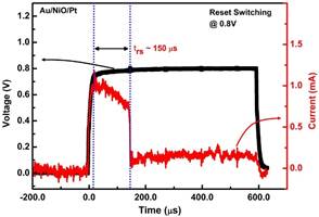 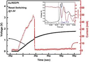
(Left) Variation in voltage pulse and current flowing through Au/NiO/Pt device during reset switching processes at reset voltage of 0.8 V, (Right) Applied voltage and current as a function of time in Au/NiO/Pt device during reset switching processes at 1.2 V. Inset shows zoomed view of variation of voltage and current with time for the reset switching.
The dynamic evolution of reset process at the reset voltage of 0.8 V is shown in figure in left. One can see that the rest process is slow with typical switching time ~ 150 µs indicating that reset process is dominated by thermally induced diffusion of point defects. To achieve fast reset switching, instead of 0.8 V reset voltage pulse, a higher amplitude voltage pulse of 1.2 V, smaller than the set voltage, was applied on device. The applied voltage pulse and current flowing through device is shown in figure in right.. It can be seen that the at the onset of reset at ~ 1.2 V the current flowing through the device dropped rapidly to smaller value corresponding to HRS. The oscillation seen in current before settling to a constant value may be due to the RC type oscillations. At the same moment the voltage applied to device also showed rapid rise nearly with the same rate as that of current. To estimate the reset time, the region containing onset of reset switching event have been enlarged as shown in inset of figure. To avoid any ambiguity in reset time estimation due to presence of RC type oscillations in current, the reset time was also measured using rise in voltage. Reset switching time of ~ 27 ns was observed when a high amplitude voltage pulse of 1.2 V is applied. Thus ns fast set and reset switching was observed in NiO thin films which is important for fast memory operations. Similar results of dynamic evolution of resistive switching with ns fast switching times was also observed for ALD grown TiO2 thin films in Au/ TiO2/Pt device configuration. In addition, we recently observed signature of quantized conductance in Al/Ta2O5/Pt devices.
Our current efforts in this area are dedicated to achieve ultra-fast (≤ns) resistive switching processes with low operating power (µW) in nanostructured metal oxides for energy efficient and fast non-volatile data storage applications.
References:
- V. K. Sahu et al., Studies on transient characteristics of unipolar resistive switching processes in TiO2 thin film grown by atomic layer deposition, J. Phys. D: Appl. Phys. 51(21), 2018, 215101-06.
- P. Misra et al., Studies on resistive switching times in NiO thin films grown by pulsed laser deposition, J. Phys. D: Appl. Phys. 50(41), 2017, 415106.
- V. K. Sahu et al., Quantized conductance in Ta2O5 based resistive random access memory devices, AIP Conf. Proc. 1832(1), 20177, 120026.
- V. K. Sahu et al., Resistive memory switching in ultrathin TiO2 films grown by atomic layer deposition, AIP Proc. 1731(1), 2016, 120032.
- G. Khurana et al., Enhanced resistive switching in forming free graphene oxide films embedded with gold nanoparticles deposited by electrophoresis, Nanotechnology, 27(1), 2015, 015702.
- Rajesh K. Katiyar et al., Unipolar resistive switching in planar Pt/BiFeO3/Pt structure, AIP Advances, 5(3), 2015, 037109.
- P. Misra et al., Resistive Switching Characteristics of Mixed Oxides, Emerging Materials Research, Emerging Materials Research4(1), 2015, 44-81.
- Geetika Khurana et al., Multilevel Resistive Memory Switching in Graphene Sandwiched Organic Polymer Heterostructure, Carbon, 76, 2014, 341-347.
- Yogesh Sharma et al., Unipolar Resistive Switching behavior of Amorphous YCrO3 Films for Nonvolatile Memory Applications, J. Appl. Phys.116(8), 2014, 084505.
- P. Misra et al., Resistance Switching and Current Conduction Mechanisms in Amorphous LaLuO3 Thin Films Grown by Pulsed Laser Deposition, Integr. Ferroelectr. 157(1), 2014, 47-56.
- P. Misra et al., Effect of Current Compliance on Resistive Switching Characteristics of Amorphous Ternary Rare Earth Oxide SmGdO3 Grown by Pulsed Laser Deposition, ECS Trans. 61(6), 2014, 133-138.
- P. Misra et al., Multilevel unipolar resistive memory switching in amorphous SmGdO3 thin film, Appl. Phys. Lett. 104 (7), 2014, 073501.
- G. Khurana et al., Forming free resistive switching in graphene oxide thin film for thermally stable nonvolatile memory applications, J. Appl. Phys. 114(12), 2013, 124508.
- P. Misra et al., On the Resistive Switching and Current Conduction Mechanisms of Amorphous LaGdO3 Films Grown by Pulsed Laser Deposition, ECS Transactions, 53(3), 2013, 229-235.
- P. Misra et al., Nonvolatile Resistive Memory Switching in Amorphous LaGdO3 Thin Films, MRS Proceedings, 1562, 2013.
- P. Misra et al., Switching Characteristics of ZnO based Transparent Resistive Random Access Memory Devices grown by Pulsed Laser Deposition, Physica Status solidi (C) 7(6), 2010, 1718.
- L. M. Kukreja et al., Studies on Nonvolatile Resistance Memory Switching in ZnO Thin Films, Bulletin of Material Science, 32(3), 2009, 247-252.
|
| |
| |
|
|
|