 FEL & Utilization Section
Research on Superconducting Materials and Superconducting Radiation Detector Elements
Structural, electric and thermo-magnetic properties V-Ti alloy superconductors: The interest in the V-Ti alloys lies in the fact that they are promising alternatives to the Nb-based superconductors for high magnetic field applications. They have excellent mechanical properties and are suitable for neutron irradiation environment. However, the lossless current carrying capability (quantified in terms of the critical current density, Jc) of the V-Ti alloys is about 2-3 orders of magnitude lower than the commercial superconductors in different magnetic fields, which the FEL&US researchers have improved in the recent years. The lossless current carrying capability of a superconductor depends on the flux line pinning properties, which in turn depends on the disorder profile. Different kinds of disorder have different efficiency of flux line pinning in different magnetic field regimes, and planned introduction of disorder is the key to improving the current carrying capability of a superconductor. However, the disorder also tends to deteriorate its mechanical properties, where the researcher has to optimize.
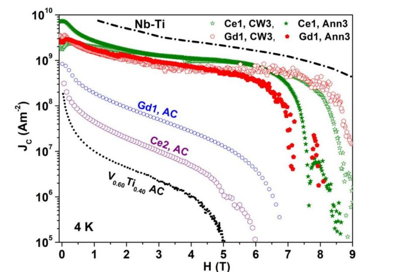
The FEL&US researchers added rare earth elements (Y, Ce, Nd, Dy, Gd) in various atomic proportions into carefully selected V-Ti alloy compositions and studied the effect of the same on the superconducting and normal state properties of V-Ti alloys. These studies show that Y is immiscible in the V-T alloy, and precipitates with various sizes during solidification from the melt. It was found that below 2 at.% Y, fine Y-rich precipitates are generated during solidification (from the melt) due to phase separation of the homogeneous V-Ti-Y liquid into a solid β-V-Ti alloy and a Y-rich liquid. The size of the Y-rich precipitates increases for higher Y content due to liquid immiscibility, and this also generates a large number of line defects. It was found that the addition of Y results in a marginal enhancement of the superconducting transition temperature due to the oxygen-scavenging effect of Y in the V-Ti matrix. The defects generated by the addition of Y were effective in pinning the flux lines and thus improving the current carrying capability. FEL&US researchers discovered a high field paramagnetic Meissner effect persisting in magnetic fields as high as 7 T, originating due to the defects created by Y addition. Correlating the structural, microstructural and flux line pinning properties in the superconducting state, the explanation behind these observations were found. It was observed that the addition of Gd is much more effective in enhancing the current carrying capability of the V-Ti alloys in spite of Gd being magnetic, and in spite of many of the Gd-added V-Ti alloys being ferromagnetic in the normal state. To understand the effect, the effects of addition of other magnetic rare earth elements like Ce, Nd, Dy on the superconducting and normal state properties of the V-Ti alloys are also being studied. It is inferred that the precipitation of rare earth elements (or their oxides) in the V-Ti matrix is a general feature, and it mostly enhances the superconducting transition temperature. Though the current carrying capability is also enhanced in this process, the tensile strength reduces drastically. By successive cold working and annealing the current carrying capability is enhanced further, especially in the high magnetic field regions. Figure 10 shows the enhancement of Jc in the V0.60Ti0.40 alloys through the process of successive cold working and annealing (SCA). This was done in the following protocol:
CW3 = C → A → C → A → C,
Ann3 = C → A → C → A → C → A,
where C = cold working to reduce the thickness to 50% each time, and A = annealing at 350, 450 or 550 or 650 C for 5 hours (based on the phase diagram). Among these three different annealing temperatures, annealing at 450 C is so far found to be the most effective in enhancing the Jc, especially in high magnetic fields. A Jc > 109 A/m2 has been achieved in 7 T field, which is close to that of the commercial Nb-Ti superconductors. The scope for further enhancement is currently being explored.
|
|
Figure 13: Enhancement of critical current density (4 K) of V0.60Ti0.40 alloys by rare earth addition and successive cold working and annealing (450 C), and comparison with commercial Nb-Ti. Here AC stands for ‘as cast’ and Ce1, Gd1, etc. indicate 1 at. % Ce or Gd content in the alloy.
|
It was also found that successive cold working and annealing results in large amount of secondary phase formation, which improves the tensile strength by 3.5 times. Moreover, by studying the normal state properties of Gd-added V-Ti alloys, evidence is found for the fact that the superconducting properties of these alloys got enhanced due to the suppression of the coherence of the spin fluctuations (inherent to the V-Ti system) by the ferromagnetic Gd precipitates. A detailed study on these spin fluctuations is currently in progress.
Research on the Development of Superconducting Radiation Detectors in the IR-FEL wavelength range: The semiconductor-based IR detectors used in the FTIR spectrometers typically use materials like InSb and HgCdTe (MCT). However, InSb-based detectors are sensitive only up to about 5.5 microns, and the Hg1-xCdxTe alloy-based (MCT) detectors are limited to about 20 microns. These detectors using semiconducting materials as the detector element have limitations in detecting long wavelengths, where the photon energies are lower than the band gap. In addition, the thermal noise resulting from their high operating temperatures also limits their use at the long wavelengths (e.g., far-IR). Superconductors, on the other hand, have much smaller energy gaps and can detect radiations up to mid-IR wavelengths with excellent sensitivity and efficiency. Carefully designed detectors using superconducting materials with even smaller energy gaps can be utilized for ultra-sensitive radiation detection in the far-IR ranges of the electromagnetic spectrum. Based on the response of the superconductors to the electromagnetic radiation, different detection schemes are employed in the superconducting radiation detectors, e.g., the kinetic inductance detectors (KIDs), superconducting nanowire single-photon detectors (SNSPDs), superconducting tunnel junctions (STJs), and transition edge sensors (TESs), etc. These detectors exhibit excellent single-photon sensitivity across a broad wavelength range varying from X-rays to millimeter waves, with (ultrafast) electronic response time down to a few picoseconds. In the FEL&US the present work focuses on the development of lumped element KIDs (LEKID) for the 12 - 50 microns wavelength range (mid and far-IR), where the IR-FEL operates. This regime is mostly unexplored and the the development of highly sensitive, broadband detectors in this wavelength range remains an open area of research.
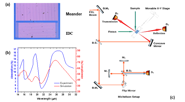
The LEKID consists of a meander structure and inter-digitated capacitors (IDCs). These two parts serve as the inductive and capacitive components respectively, and determine the geometrical resonance frequency of the structure. The optical efficiency of the LEKID geometry depends on the normal state resistivity of the superconducting material, dielectric constant of the substrate, and the width of the meander lines and their spacing in-between. After identifying the superconducting element-material through experimental studies on the material properties and electromagnetic (CST) simulations, and then again simulating the light absorption in the LEKID geometry obtained using such materials, the LEKID structures are designed and then fabricated. One such superconducting Ti40V60 alloy thin film structure, synthesized in-house using UHV based pulsed DC magnetron sputtering technique combined with UV-photolithography followed by a lift-off process (to deposit the thin film in the LEKID pattern), is shown in figure 14(a). In the image, the meander portion (meander line width = 6 m and meander pitch =12 m) is the effective radiation-sensitive portion, and the IDCs are used for tuning the resonance frequency of the designed LEKID structure. Simultaneous transmission and reflection measurements were performed using the IR-FEL light for the experimental estimation of the absorption in the fabricated geometry. The corresponding intensities were recorded using pyroelectric detectors, and the wavelength of the IR-FEL light was measured using the Michelson interferometer at port P-4. Due to the near-continuous wavelength tunability of the IR-FEL, these measurements revealed the wavelength-dependent absorption characteristics of the LEKID structure. Figure 14(b) shows the absorption in the above mentioned LEKID structure at different wavelengths ranging from 14 to 30 microns, in comparison with the results from CST simulation with the experimentally measured absorption using IR-FEL light. Figure 14(c) shows the schematic diagram of the absorption measurement set-up near port P-4. While the trends seen in the experimental curve of figure 14(b) does match with the simulation, further studies are currently in progress to appropriately configure the back short distance and resonator geometry in these detector structures to ultimately achieve a high light absorption of > 95%.
|
|
Figure 14: (a) Superconducting Ti40V60 alloy thin film based LEKID structure synthesized using pulsed DC magnetron sputtering and UV-photolithography. (b) Comparison of experimentally measured absorption in the LEKID structure with the results from CST simulations at different IR-FEL wavelengths ranging from 14 to 30 microns. (c) Schematic diagram of the experimental set-up at port P-4, used for for the estimation of absorption through simultaneous measurements of IR-FEL light transmission and reflection.
|
|