The Angle Resolved Photo Electron Spectroscopy (ARPES) beamline has been set up on Indus-1 synchrotron radiation source (SRS). The experimental station of the beamline is equipped with a 5 axis cryo manipulator, a separate sample preparation chamber, and pulsed laser deposition (PLD) system and to facilitate the in-situ PES studies of solid samples including thin films. Measurements can be performed in Angle Integrated mode on thin films and pellet samples.
Parameters
Parameter
Pre-mirror
Post-mirror
TGM
Acceptance (mrad)
8.9 (H) x 5.2 (V)
14.3 x 8.8
20 x 12.4
Entrance Arm Length (mm)
3400
1102
1000
Exit Arm Length (mm)
1500
1155
1414
Angle Of Incidence
85.5°
85.5°
162°
Meridional Radius, R (mm)
26732
14380
7977
Sagittal Radius (mm)
165
88.5
182.3
Demagnification Ratio
2.3: 1
0.95: 1
Size (mm × mm)
240 × 30
115 × 15
75 × 20
Coating
Pt
Pt
Pt
Gratings
Grating 1 (1800 Grooves/mm)
Grating 2 (600 Grooves/mm)
Grating 3 (200 Grooves/mm)
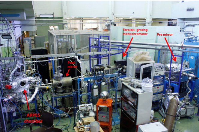
Photograph of the Beamline showing various components:
Experimental station
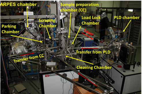
The experimental station is capable of recording Angle integrated PES spectra on solid/thin film samples using PHOIBOS-150 electron analyser equipped with MCP based CCD detector. A view of the corresponding experimental station is shown in the figure below. The analysis chamber (mu-metal) is equipped with a cryo sample manipulator, which is useful to position the sample and record the data from room temperature down to ~6 K. The ARPES system also has a twin-anode (Al, Mg) X-ray lab source for XPS (ESCA) studies, Helium discharge lamp for high resolution valence band PES. The overall experimental energy resolution of the beamline is in the range of 140 meV- 400 meV. A dedicated sample preparation chamber for sample cleaning is attached to the ARPES analysis chamber. In this chamber, samples cleaning facilities like cleaving, scrapping, annealing (up to 800° C) and Ar+ ion sputter gun are mounted to ensure the contamination free samples for the measurements. A load-lock chamber is attached to the sample preparation chamber, which enables quick transfer of the sample from atmosphere. The UHV parking for 5 samples is also provided. The sample size, which can be accommodated on the sample holder, is of area 10 mm x10 mm (maximum) with 0.5 mm thickness. The type of the samples that can be taken up for studies on this beamline should be of non-volatile and UHV compatible solids in thin/thick films or pellet form.
Photograph of the ARPES experimental station:
Features
Electron analyser: PHOIBOS-150 (150 mm mean radius)
Electron detector: MCP based 2D CCD detector, capable for AIPES & Angular resolved PES Measurements
Sample manipulations: X-Y-Z-θ (rotation) and φ (azimuthal)
Vacuum in analysis chamber: < 5x10-11 mbar.
Incident flux monitoring: Online normalization of photon flux by sample ground Current/ post mirror ground current.
Flood gun for charge compensation.
Sample temperature range: Room temperature to 6 K.
In-situ growth facility for thin films using Pulsed laser deposition (Q-switched Nd:YAG laser, 1064, 532, 355 and 266 nm wavelengths, Target-Substrate distance: 5 cm, Substrate heating up to 800° C)
Sample Loading: Quick accessed load lock facility for loading three sample simultaneously
Sample preparation: Ar+ ion Sputtering, cleaving, scrapping & annealing facility (27 °C – 800 °C)
Sample parking: 5 samples can be parked under UHV environment (<5x10⁻¹⁰ mbar)
Residual gas analyser in ARPES chamber for detecting the presence of various gases inside the chamber
Application Areas
Spectroscopy of buried interfaces
Elemental composition
Chemical state information
Band offset measurement of hetro-junction
Work function measurement
Functional materials, phase transition studies as a function of temperature
1.
Effect of phase transition on structural, dielectric, and electrical properties of pulsed laser deposited Y doped high k HfO2 thin films M. Nand, P. S. Padhi, S. Tripathi, Y. Kumar, P. Sahu, M. Kumar, A. Dawar, S. Ojha, P. Misra, H. Srivastava, S. K. Rai
J. Vac. Sci. Technol. A 43 (2025) 023411.
2.
Structural, electrical, and magnetic properties of (1-x)ZnFe2O4-(x)BaTiO3 (x = 0,0.05,0.10,1) system H. Cheema, P. A. Al, J. Tanwar, P. Kushwaha, S. N. Jha, S. Tripathi, U. Kumar,
J. Australian Ceramic Society (2025) https://doi.org/10.1007/s41779-025-01219-7
1.
Resonance photoemission in pure and Tb doped CePO4 luminescent nanowires S. Tripathi, Y. Kumar, M. Nand, M. Baral, A. Sharma, H. Shrivastava, S. Raj Mohan, R. Singh, R. Jangir, U. Deshpande, S.N. Jha
Journal of Alloys and Compounds 994 (2024) 174617.
2.
Effect of oxygen partial pressure on phase, local structure and photoluminescence properties of Hf(1-x)YxO2 thin films prepared by pulsed laser deposition M. Nand, P. Rajput, S. Tripathi, M. Kumar, Y. Kumar, H. Bhatt, P. Deshmukh, H. Srivastava, S. K. Mandal, R. Urkude, S. Satapathy, M. Gupta and S.N. Jha
Vacuum 221 (2024) 112882.
1.
Influence of ion irradiation on the surface electronic structure of epitaxial lanthanum nickelate films V. Sharma, I. Singh, Sunidhi, S. K. Arora, F. Sanchez, F. Singh, S. Tripathi, S. N. Jha,
Surfaces and Interfaces 38 (2023) 102776.
1.
Different polymorphs of Y doped HfO2 epitaxial thin films: Insights into structural, electronic and optical properties M. Nand, S. Tripathi, P. Rajput, M. Kumar, Y. Kumar, S. K. Mandal, R. Urkude, M. Gupta, A. Dawar, S. Ojha, S.K. Rai and S.N. Jha,
J. Alloy. Comp., 928 (2022) 167099.
2.
Determination of band alignment in liquid exfoliated few-layer WSe2/SiO2 interface Rahul, S. K. Arora, S.N. Jha, Yogesh Kumar, Materials Letters, 311 (2022) 131600.
3.
Band gap engineering of TiO2 by Mn doping and the effect of p-TNT:Mn/n-MnO2 heterojunction on photocatalytic applications P. S. Nair, H. Rahman, J. A. Joseph, A. Norbert, S. Shaji, S. Tripathi, S. N. Jha, R. R. Philip,
Applied Physics A, 128 (2022) 1089.
4.
Impact of Atomic Rearrangement and Single Atom Stabilization on MoSe2@NiCo2Se4 Heterostructure Catalyst for Efficient Overall Water Splitting A. Majumdar, P. Dutta, A. Sikdar, H. Lee, D. Ghosh, S. N. Jha, S. Tripathi, Y. Oh and U. N. Maiti,
Small 18 (2022) 2200622.
5.
Electronic structure of rare-earth semiconducting ErN thin films determined with synchrotron radiation photoemission spectroscopy and first-principles analysis K. Upadhya, R. Kumar, M. Baral, S. Tripathi, S. N. Jha, T. Ganguli and B. Saha,
Physical Review B 105 (2022) 075138.
6.
Band alignment determination in few-layer exfoliated MoSe2/SiO2 interface using Synchrotron-based photoemission spectroscopy Rahul, S. K. Arora, S. N. Jha, Y. Kumar,
Eur. Phys. J. Plus, 137 (2022) 666.
7.
Electronic structure modification in Fe-substituted β-Ga2O3 from resonant photoemission and soft x-ray absorption spectroscopies S. Ghosh, M. Nand, R. Kamparath, M. Gupta, D. M. Phase, S. N. Jha, S. D. Singh and T. Ganguli,
J. Phys. D: Appl. Phys. 55 (2022) 185304.
8.
Spin reorientation transition driven by polaronic states in Nd2CuO4 S. Banik, K. Vijaya, S. Paul, N. Mansuri, D. K. Shukla, S. K. Srivastava, A. Sagdeo, K. Kumar, S. Tripathi, S. N. Jha,
Mater. Adv., 3 (2022) 7559-7568.
9.
Structural, optical and vacancies investigations of Li-doped ZnO P. Rajput, M. Kumar, R. S. Joshi, P. Singh, M. Nand, R. Srivastava, Y. Patidar, S. Kumar, A. Sagdeo, P. R. Sagdeo, M. Gupta, F. Singh, S. A. Khan, P. Mondal, A. K. Srivastava, D. Bhattacharyya, S. N. Jha,
J Nanopart Res 24 (2022) 161.
10.
Wide-Band-Gap p-Type GaCrO3:Ni Semiconductor: A Hole Transport Material R. Jangir, V. Srihari, A. Kumar Bhakar, M. Nand, D. K. Shukla, S. N. Jha, and T. Ganguli,
ACS Appl. Energy Mater. 5 (2022) 8629–8638.
1.
Development of UHV pulsed laser deposition set-up for in-situ photoelectron spectroscopic study at ARPES beamline, Indus-1 synchrotron radiation source, India M. Nand, Y. Kumar, A. Dwivedi, S. Tripathi, Babita, R. J. Choudhary, S. N. Jha,
Nuclear Inst. and Methods in Physics Research A 986 (2021) 164805.
1.
Large positive magnetoresistance and Dzyaloshinskii–Moriya interaction in CrSi driven by Cr 3d localization S. Banik, M. K. Chattopadhyay, S. Tripathi, R. Rawat and S. N. Jha,
Scientific Reports 10 (2020) 12030.
2.
Structural and optical properties of transparent, tunable bandgap semiconductor: α-(AlxCr1−x)2O3 R. Jangir, V. Srihari, A. Bhakar, C. Kamal, A. K. Yadav, P. R. Sagdeo, D. Kumar, S. Tripathi, S. N. Jha and T. Ganguli,
J. Appl. Phys. 128 (2020) 135703.
3.
Study of valence band electronic states of near-surface atoms of niobium used for superconducting cavity N. Singh, Mangla Nand, S. N. Jha, S. Raghavendra,
Journal of Electron Spectroscopy and Related Phenomena 420 (2020) 146942.
4.
Crystalline Bi2Se3 topological insulator films prepared by DC magnetron sputtering R. Kumar, A. K. Yadav, A. Biswas, Mangla Nand, J. Bahadur, S. Ghosh, S. N. Jha, D. Bhattacharyya,
Vacuum 177 (2020) 109366.
5.
Investigations on epitaxy and lattice distortion of sputter deposited β-Ga2O3 layers on GaN templates Sahadeb Ghosh, Himanshu Srivastava, P. N. Rao, Mangla Nand, Pragya Tiwari, A. K. Srivastava, S. N. Jha, S. K. Rai, S. D. Singh, and Tapas Ganguli,
Semiconductor Science and Technology 35 (2020) 085024.
6.
Si compatible MoO3/MoS2 core-shell quantum dots for wavelength tunable photodetection in wide visible range S. Pal, S. Mukherjee, M. Nand, H. Srivastava, C. Mukherjee, S. N. Jha, and S. K. Ray,
Applied Surface Science 502 (2020) 144196.
1.
Electrical and optical properties of low-bandgap oxide Zn2Mo3O8 for optoelectronic applications P. Ravindra, M. Baral, T. Biswas, M. Nand, S. N. Jha, E. Athresh, R. Ranjan, M. Jain, T. Ganguli, S. Ivasthi,
Thin Solid Films 677 (2019) 95–102.
1.
Studies on structural and optical gap tunability in α-(GaxCr(1-x))2O3 solid solutions R. Jangir, D. Kumar, V. Srihari, A. Bhakar, A. K. Poswal, P. R. Sagdeo, M. Nand, S. N. Jha, P. Tiwari, T. Ganguli,
Journal of Alloys and Compounds 766 (2018) 876–885.
1.
Epitaxial growth and band alignment properties of NiO/GaN heterojunction for light emitting diode applications K. Baraik, S. D. Singh, Yogesh Kumar, R. S. Ajimsha, P. Misra, S. N. Jha, and T. Ganguli,
Applied Physics Letters 110 (2017) 191603.
2.
Band alignment and charge transfer pathway in three phase anatase-rutile-brookite TiO2 nanotubes: An efficient photocatalyst for water splitting L. K. Preethi, T. Mathews, M. Nand, S. N. Jha, C. S. Gopinath, S. Dash,
Applied Catalysis B: Environmental 218 (2017) 9–19.
3.
Effect of dry air on interface smoothening in reactive sputter deposited Co/Ti multilayer A. Biswas, A. Porwal, D. Bhattacharya, C. L. Prajapat, A. Ghosh, M. Nand, C. Nayak, S. Rai, S. N. Jha, M. R. Singh, D. Bhattacharyya, S. Basu and N. K. Sahoo,
Applied Surface Science 416 (2017) 168–177.
1.
Electronic Structure of FeAl Alloy Studied by Resonant Photoemission Spectroscopy and Ab Initio Calculations D. Mondal, S. Banik, C. Kamal, M. Nand, S. N. Jha, D. M. Phase, A. K. Sinha, A. Chakrabarti, A. Banerjee, T. Ganguli,
Journal of Alloys and Compounds 688 (2016) 187.
2.
Interface structure in nanoscale multilayers near continuous-to-discontinuous regime P. C. Pradhan, A. Majhi, M. Nayak, M. Nand, P. Rajput, D. K. Shukla, A. Biswas, S. K. Rai, S. N. Jha, D. Bhattacharyya, D. M. Phase, and N. K. Sahoo,
Journal of Applied Physics 120 (2016) 045308.
3.
Raman and photoelectron spectroscopic investigation of high-purity niobium materials: Oxides, hydrides, and hydrocarbons N. Singh, M. N. Deo, M. Nand, S. N. Jha, and S. B. Roy,
Journal of Applied Physics 120 (2016) 114902.
4.
Determination of band offsets at strained NiO and MgO heterojunction for MgO as an interlayer in heterojunction light emitting diode applications S. D. Singh, M. Nand, R. S. Ajimsha, A. Upadhyay, R. Kamparath, C. Mukherjee, P. Misra, A. K. Sinha, S. N. Jha, and T. Ganguli,
Applied Surface Science 389 (2016) 835.
5.
Structural, electronic structure, and band alignment properties at epitaxial NiO/Al2O3 heterojunction evaluated from synchrotron based X-ray techniques S. D. Singh, M. Nand, A. Das, R. S. Ajimsha, A. Upadhyay, R. Kamparath, D. K. Shukla, C. Mukherjee, P. Misra, S. K. Rai, A. K. Sinha, S. N. Jha, D. M. Phase, and T. Ganguli,
Journal of Applied Physics 119 (2016) 165302.
1.
Ultraviolet photoelectron spectroscopy of nano In clusters Schottky barriers on sputtered InP S. Kumar, C. Mukherjee, V. K. Dixit, S. D. Singh and S. N. Jha,
Applied Surface Science 258 (2011) 143–146.
2.
Electronic structure of CeAg2Ge2 studied by resonant and angle-resolved Photoemission Spectroscopy S. Banik, S. K. Deb, A. Chakrabarti, A. Thamizhavel, D. M. Phase and S. N. Jha,
Diamond Light Source Proceedings 1 (2011) e138, page 1 (SRMS-2011).
1.
Optical and X-ray photoelectron Spectroscopy of PbGeO3 and Pb5Ge3O11 single crystals S. C. Sabharwal, S. N. Jha and Sangeeta,
Bulletin of Material Science 33 (2010) 395–400.
2.
Band Mapping of CeAg2Ge2 using Angle-resolved photoemission spectroscopy S. Banik, A. Chakrabarti, S. K. Deb, S. N. Jha, S. V. N. B. Rao, D. A. Joshi, A. Thamizhavel and S. K. Dhar,
Solid State Communications 150 (2010) 1936–1939.
1.
Valence band electronic structure of Pr1-xSrxMnO3 from photoemission studies P. Pal, M. K. Dalai, B. R. Sekhar, S. N. Jha, S. V. N. Rao, N. C. Das, C. Martin and F. Studer,
Journal of Physics: Condensed Matter 17 (2005) 2993.
1.
Valence bands offset between depleted semiconductors measured by photoelectron spectroscopy S. Kumar, S. N. Jha, Jagannath, T. Ganguli, S. V. N. B. Rao, N. C. Das,
Applied Surface Science 229 (2004) 324–332.
1.
Development of Angle Resolved Photoelectron Spectroscopy Beamline at Indus-1 Synchrotron Radiation Source N. C. Das, S. N. Jha, S. V. N. B. Rao, B. N. Rajasekhar, S. S. Bhattacharya, S. K. Sikka, Jagannath, A. V. Korgaonkar, K. G. Bhushan, J. V. Yakhmi, and V. C. Sahani,
Journal of Optics, India 32 (2003) 27.
Science Highlights
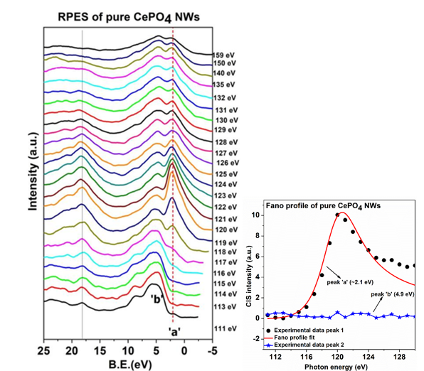
RPES studies on Tb:CePO4 nanowires prepared using green synthesis chemical route.:
The relative participation of ce3+ and ce4+ oxidation states in the valence band and effect of Terbium, are important factors in defining the optical properties that determine the photoluminescence (PL) intensity. The RPES experiments performed around the Ce 4d →4f resonance threshold at the beamline indicated strong presence of ce3+ (Ce 4f) states in pure CePO4 NWs, which reduced upon Tb doping due to efficient doping of Tb and strong energy transfer from ce3+ to Tb3+ ions. The results were supported by high PL emission intensity in the visible wavelength range indicating strong green luminescence due to efficient ce3+ to Tb3+ energy transfer.
Figure: RPES data showing the enhancement of ce3+ contribution (peak ‘a’) while the contribution from ce4+ oxidation state (peak ‘b’) remains constant. Corresponding Fano profile fitting revealed strong resonance effect in ce3+ oxidation state, while no resonance in ce4+ oxidation state
Ref: S. Tripathi et. al, J. Alloy . Comp. 994 (2024) 174617.
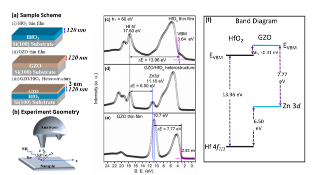
In-situ valence band offset measurement of PLD grown GZO/HfO2 heterostructure using PES :
Nd:YAG laser based UHV PLD system was developed at ARPES beamline. The system was used to prepare GZO/HfO2 heterostructure and the band offset of GZO/HfO2 heterostructure was investigated by in-situ PES measurements using synchrotron radiation. The film surface is found to be contamination free, which demonstrates the capability of the set-up for in-situ PES studies The Hf 4f and Zn 3d core level peaks along with valence band maxima positions were used to determine the valence band offset. The valence band offset was found to be 0.31 ± 0.08 eV, which is the first result reported on this heterostructure system. The capability of the present set-up can be extended in future by adding RHEED, STM etc.
Figure: (a) The deposited sample scheme for band offset calculation using in-situ PES measurements, (b) PES experimental geometry, (c), (d) & (e) are in-situ PES spectra recorded with 60 eV photon energy from SR source. (c) Hf 4f core level and valence band maxima (VBM) measured on HfO2 thin film, (d) Hf 4f core level and Zn 3d energy level measured on GZO/HfO2 heterostructure thin film, (e) Zn 3d energy level and valence band spectra from GZO thin film, and (f) the band alignment diagram for GZO/HfO2 heterostructure.
Ref: Mangla Nand et. al, Nuclear Inst. and Methods in Physics Research A, 986 (2021) 164805.