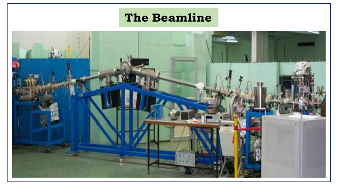
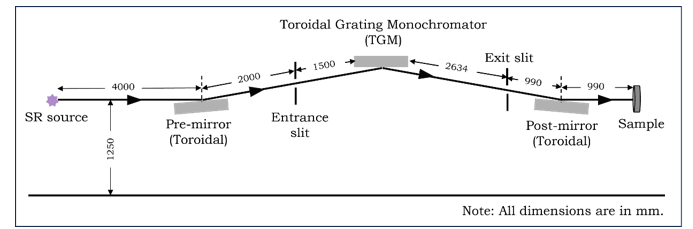
Angle integrated photoelectron spectroscopy (AIPES) beamline is designed to utilize photons in the energy range from 10 to 200 eV. The beamline operates at a vacuum better than 10-9 mbar. The basic requirements for carrying out the photoemission experiments are good photon flux and moderate resolution. Since toroidal grating monochromator (TGM) fulfil these two requirements, the present beamline is developed around it.
In order to have good reflectivity in this energy range, a grazing incidence-reflecting optics is used.
A toroidal pre-mirror which is kept at a distance 4000 mm from the source accepts radiation over horizontal and vertical acceptance angles of 10 and 2.5 mrad respectively.
The grazing angle of incidence at the mirror is about 4.5°, giving a deviation of 9° after reflection.
The reflected beam is brought to a focus at a distance of 2000 mm where the entrance slit of TGM is located.
The pre-mirror section is followed by a TGM (Jobin Yvon-TGM2634) which contains three interchangeable gratings to cover a photon energy range from 10 to 200 eV.
Monochromatized beam passing through an exit slit falls on post-focusing toroidal mirror.
Pt-coated post mirror refocuses the monochromatic beam from exit slit to a sample located at 990 mm with magnification 1:1.
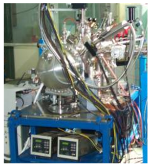
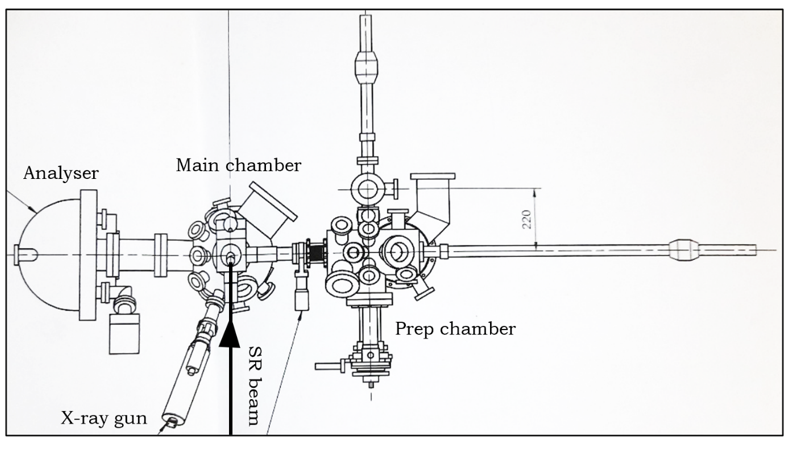
Experimental station
The main components and schematic of the AIPES end-station are given below:
Main Components
Omicron hemispherical energy analyser (EA-125, Germany)
Probing photo-assisted charge storage mechanism using Bi-Fe perovskite oxide electrode for solar supercapacitor.
Manopriya Samtham, Ajay Patil, Ekta Choudhary, Himanshu Srivastava, Ravindra Jangir, R.J. Choudhary, and Rupesh S Devan;
Small Methods 9 2401441 (2025).
2.
Revealing the Role of Fe and Ti in the Quest for Different Magnetic Ordering in Double Perovskite Sr2FeTiO6.
Divya Kumari, Digvijay Narayan Singh, Sourav Chowdhury, R. J. Choudhary, and Seema Sharma;
Mater. Chem. Phys. 334 130411 (2025).
3.
Synthesis and Spectroscopic Investigations of Sm3+ Activated ZrO2 and Na2ZrO3 as Warm Light Phosphors.
P Khajuria, VD Sharma, A Khajuria, R Prakash, and R.J. Choudhary;
J. Fluoresc. 35 2023 (2025).
4.
Synthesis, structure and magnetic properties of Pr3Ni2NbO9 double perovskite.
R. Athira, Yogesh Kumar, D.P. Sahu, A.K. Singh, R.J. Choudhary and S.D. Kaushik;
Ceram. Int. 51 8758 (2025).
5.
Anti-site Disorder Driven Unusual Magnetic Properties in Sm2NiMnO6 Double Perovskite.
S. Majumder, S. Saha, Malvika Tripathi, P. Rajput, SN Jha, R. J. Choudhary, and D. M. Phase;
J. Supercond. Nov. Magn. 38 29 (2025).
6.
Structural and magnetic evolution in Ga3+-doped DyMnO3: Impact on Jahn-Teller distortion and spin glass behaviour.
Paresh Siddhpura, Tanvi Dudharejiya, Nirali Udani, Sandhya Dodia, Gaurav Jadav, D.K. Dhruv, Sergei A. Sharko, J.H. Markana, R.J. Choudhary, and Bharat Kataria;
Cer. Int. in press (2025).
7.
Optoelectronic properties of Na2ZrO3: Eu3+ phosphor: Judd-Ofelt insights and applications in solid-state lighting and latent fingerprinting.
Pooja Khajuria, Vishav Deep Sharma, Ishant Kumar, Arti Khajuria, Ram Prakash, RJ Choudhary;
J. Alloys Compds. 1025 180268 (2025).
8.
Role of crystal structure and local electronic structure on the magnetic behaviour of DyMn1−xFexO3 (x = 0.0, 0.3, 0.5, 0.7, and 1.0) system.
Urjitsinh Rathod, Sumana Hajra, Sadaf Jethva, Savan Katba, Megha Vagadia, Rajashri Urkude, RJ Choudhary, M Gupta, Ashish Ravalia;
Journal of Alloys and Compounds. 183667 (2025).
9.
Probing half-metallicity in Mn2CoSi/Si(100) thin film structures using electrical transport measurements towards spintronic applications.
Anadi Krishna Atul, Indra Sulania, R. J. Choudhary, and Neelabh Srivastava;
J. Phys. Chem. Solids. 196 112391 (2025).
10.
Effect of Fe doping on the electronic properties of CoSn Kagome semimetal.
Kritika Vijay, Kawsar Ali, Najnin Bano, Anju Ahlawat, Mukul Gupta, R.J. Choudhary, D K Shukla, Ashok K Arya and Soma Banik;
J. Phys. Cond Matt. 37 095502 (2025).
1.
Activation of KZr2(PO4)3 nanophosphor with Dy3+ to demonstrate its optical and spectral properties.
VD Sharma, P Khajuria, A Khajuria, R Prakash, and RJ Choudhary;
J. Electr. Mat. 1–14 (2024).
2.
To study structural morphological and ferromagnetic behaviour of Sn1−xMnxO2 thin films.
V Rathore, P Gupta, K Sharma, and RJ Choudhary;
Chem. Phys. Lett. 852 141476 (2024).
3.
Role of competing magnetic anisotropies in deriving topologically nontrivial spin textures in oxide heterostructures.
Jayaprakash Sahoo, Megha Vagadia, René Hübner, Neeraj Bhatt, Ankit Kumar, Ganesh Sahastrabuddhe, R. J. Choudhary, Ravi Shankar Singh and D. S. Rana;
Phys. Rev. B 110, 104422 (2024).
4.
Competing s-p and p-p fluctuations in charge-disproportionation of BaBiO3.
Sumit Sarkar, R.J. Choudhary, Manju Sharma and Rajamani Raghunathan;
Adv. Theory Simul. 7 2400328 (2024).
5.
Photoluminescent and X-ray photoemission studies of Eu3+-doped kosnarite KZr2(PO4)3 nanophosphor and its Judd–Ofelt analysis.
VD Sharma, P Khajuria, A Khajuria, R Prakash, and RJ Choudhary;
J. Nanoparticle Res. 26, 1 (2024).
6.
La implanted band engineering of ZnO nanorods for enhanced photoelectrochemical water splitting performance.
Santosh Bimli, Sameena R. Mulani, Ekta Choudhary, Aayushi Miglani, Pratibha Shinde, Sandesh R. Jadkar, R.J. Choudhary, and Rupesh S. Devan;
Int. J. Hydrogen Energy 71 227 (2024).
7.
Magnetic anomaly in CoCr2O4−δ.
Nausheen Noor, Anita Bagri, Sumit Sarkar, Koushik Dey, Binoy Krishna De, Vasant Sathe, R.J. Choudhary and Ashutosh Mishra;
J. Mag. Mag. Mater. 600 172131 (2024).
8.
Low-Intensity Light Detection with a High Detectivity Using 2D-Sb2Se3 Nanoflakes on 1D-ZnO Nanorods as Heterojunction Photodetectors.
Santosh Bimli, Vishesh Manjunath, Sung Hyeon Jung, Dong Su Kim, R.J. Choudhary, Ravindra Jangir, Himanshu Srivastava, Shailesh Rana, Hyung Koun Cho, Rupesh S Devan and Nishad G Deshpande;
ACS Appl. Mat. & Interf. 16 31261 (2024).
9.
A-site heterovalency induced cationic disorder effects on the structural, electronic, and magnetic properties of double perovskite: Sr2FeMnO6.
Divya Kumari, Digvijay Narayan Singh, Sourav Chowdhury, Md.K. Shamim, R.J. Choudhary and Seema Sharma;
J. Alloys Compd. 987 174079 (2024).
10.
Manganese substitution effect on physical properties of sol-gel derived DyFeO3 orthoferrite.
Abhijeet Kumar, Siddhartha Swarup Parida, RJ Choudhary, N Vijayan, and Budhendra Singh;
Mater. Chem. Phys. 319 129365 (2024).
11.
Tuning the structural and electronic characteristics of La0.07Sr0.93SnO3 thin films through co-doping with antimony.
Y. Kumar, R.J. Choudhary and A.P. Singh;
Ceramics International 50 14340 (2024).
12.
The borophene quantum dots anchored TiO2 nanocomposite as an efficient photo electrocatalyst for water splitting application.
H. J. Yashwanth, K. Hareesh, R. J. Choudhary, and Sanjay D. Dhole;
Appl. Surf. Sc. 646 158910 (2024).
1.
Memristive Thermal Switching in Epitaxial V2O3 Thin film.
Sophia Sahoo, Hemant Singh Kunwar, Satish Yadav, Rajeev Rawat, Vasant Sathe, D.M. Phase and Ram Janay Choudhary;
J. Alloys Compd. 970 172620 (2023).
2.
Observation of room temperature ferromagnetism in transition metal ions substituted p-type transparent conducting oxide Cr2O3 thin films.
P Bhardwaj, J Singh, AP Singh, RJ Choudhary, V Verma, R Kumar;
Mater. Sci. Eng. B 299, 116990 (2024).
3.
Role of structural, morphological, and electronic characteristics in investigating the low temperature transport and magnetic behavior of Sr doped Sm2NiMnO6.
Shohaib Abass, Khalid Sultan, Sujoy Chakravarty, and R.J. Choudhary;
J. Alloys Compd. 968 172191 (2023).
4.
Study of the synergistic role of multivalence states of 3d cations on the crystal lattice distortion and magnetic behavior of Sr2FeCoO6-δ: A spectroscopic study.
Divya Kumari, Digvijay Narayan Singh, Md. K. Shamim, Sourav Chowdhury, R. J. Choudhary and Seema Sharma;
J. Alloys Compd. 968 171768 (2023).
5.
Visible light-driven photocatalyst δ-Bi7VO13 nanoparticles synthesized by thermal plasma.
Shankar S. Kekade, Suyog A. Raut, Ram J. Choudhary, Trupti S. Barve, Vikas L. Mathe, Deodatta M. Phase, Damien Thiry, and Shankar I. Patil;
J. Mater Sci: Mater Electron 34 2326 (2023).
6.
Electronic comprehension of exchange bias effect in Sr2CoRuO6-δ thin-film.
Subho Saha, Anita Bagri, Sourav Chowdhury, Priyanka Yadav, and Ram Janay Choudhary;
J. Appl. Phys. 134, 185301 (2023).
7.
A novel yellow whitish Dy3+ activated NaZr2(PO4)3 phosphor: Structural, spectral and optical investigations.
Vishav Deep Sharma, Pooja Khajuria, Sandeep Kumar, Ram Prakash, and R.J. Choudhary;
Optik 291 171354 (2023).
8.
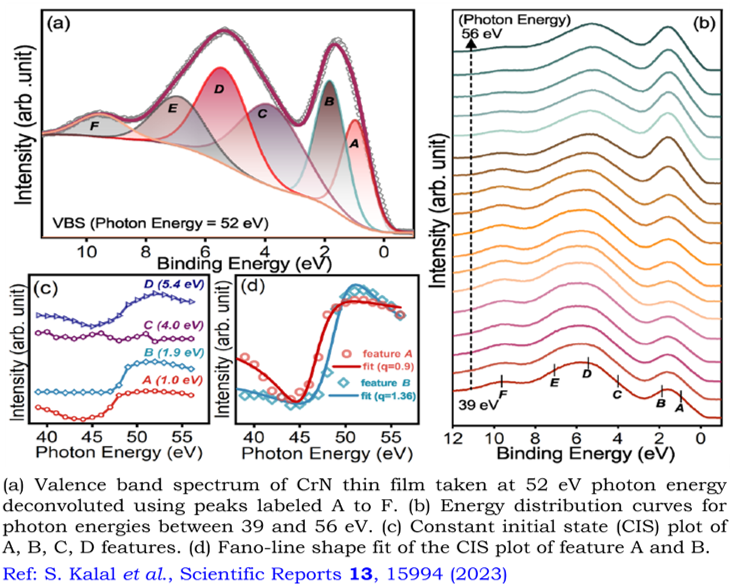
Electronic correlations in epitaxial CrN thin film.
Shailesh Kalal, Sanjay Nayak, Sophia Sahoo, Rajeev Joshi, Ram Janay Choudhary, Rajeev Rawat and Mukul Gupta;
Scientific Reports 13, 15994 (2023).
9.
Investigating Magnetic and Magneto-Transport Properties of Ferromagnetic (FM) structure and Antiferromagnetic/Ferromagnetic (AFM/FM) heterostructures.
Pooja Narwat, R J Choudhary∗ and A Mishra;
Physica B 665, 415048 (2023).
10.
Synthesis and Luminescence Properties of High-Purity Red-Light-Emitting Eu3+-Doped NaZr2(PO4)3 Phosphor.
VD Sharma, P Khajuria, R Prakash, RJ Choudhary;
J. Electr. Mat. 52, 6146 (2023).
11.
Visible-light controlled interfacial magnetoelectric coupling in SrRuO3/BaTiO3 heterostructure.
Anita Bagri, D. M. Phase and R. J. Choudhary;
Acta Materiala 255 119091 (2023).
12.
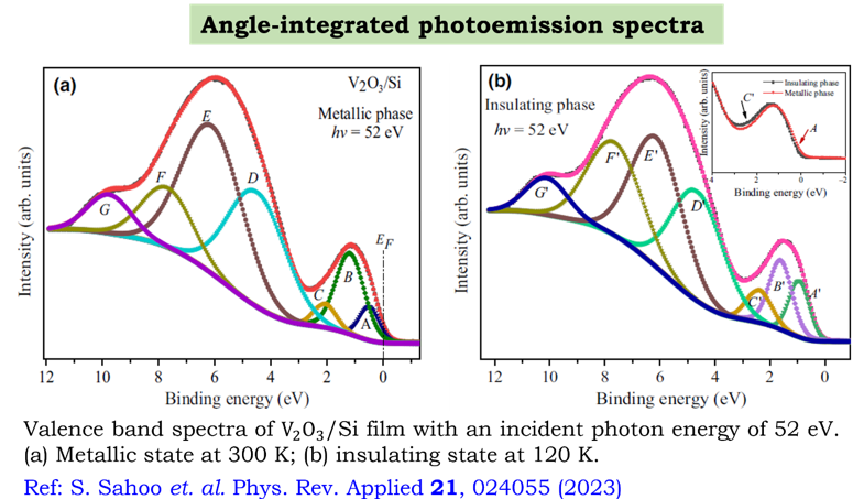
Electrically induced resistive switching in V2O3/Si thin film.
Sophia Sahoo, Anupam Jana, Satish Yadav, Rajeev Rawat, D. M. Phase, and R. J. Choudhary;
Phys. Rev. Appl. 20, 024055 (2023).
13.
Influence of Sm3+ ion doping on the surface and photoluminescence properties of Ba3Zr2O7 phosphor.
Pooja Khajuria, Vishav Deep Sharma, Rubby Mahajan, Ram Prakash, and R.J. Choudhary;
Materials Today Comm. 36 106373 (2023).
14.
Intermediate valence and spin fluctuations near a quantum critical point in CeRu2−xCoxGe2.
Swati Pandey, Ashish Kumar Mishra, M. P. Saravanan, P. K. Biswas, A. K. Yadav, S. N. Jha, D. Bhattacharyya, R. J. Choudhary, R. Rawat and V. Siruguri;
Phys. Rev. B 108 014407 (2023).
15.
Influence of Bi3+ Substitution on the Structural and Magnetic Properties of Pr0.6Sr0.4MnO3 Ceramics.
Anita D Souza, Megha Vagadia, Sujay Chakravarty, Jayaprakash Sahoo, R. J. Choudhary, Sudhindra Rayaprol, Mamatha D. Daivajna;
J. Mag. Mag. Mater. 576 170692 (2023).
16.
Qualitative study of structural phase transition in nickel doped La2CoTi(1−x)NixO6 double perovskite.
Neha Solanki, R.J. Choudhary and Netram Kaurav;
J. Alloys Compd. 943 169126 (2023).
17.
Photonically Cured Solution-Processed SnO2 Thin Films for High-Efficiency and Stable Perovskite Solar Cells and Minimodules.
Nisha Sarda, Arya Vidhan, Susmita Basak, Preetam Hazra, Tejmani Behera, Sudeshna Ghosh, R J Choudhary, Arindam Chowdhury, and Shaibal K. Sarkar;
ACS Appl. Energy Mater. 6 3996 (2023).
18.
Role of local structural distortions on the origin of j=1/2 pseudo-spin state in sodium iridate.
Priyanka Yadav, Sumit Sarkar, Manju Sharma, DM Phase, R J Choudhary, Rajamani Raghunathan;
ACS Appl. Electronic Mat. 5 418 (2023).
19.
Evolution of valence state of Ru metal ions in correlation with the structural and electronic properties of double perovskite ruthenates; A2SmRuO6 (where A = Ba & Sr).
Sahil Dani, Rabia Pandit, Hitesh Sharma, A. Arya, R J Choudhary, Navdeep Goyal, Jarnail Singh, and Rakesh Kumar;
J. Mater. Chem. C 11 4081 (2023).
20.
Integrated experimental and theoretical studies on structural and magnetic properties of thin films of double perovskite ruthenates Ba2DyRuO6 & Sr2DyRuO6.
Sahil Dani, Rakesh Kumar, Hitesh Sharma, R J Choudhary, Navdeep Goyal, Pawanpreet Kaur, and Rabia Pandit;
Phys. Chem. Chem. Phys. 25 20863 (2023).