The Grazing Incidence X-ray Scattering Beamline (BL-13) at Indus-2 was designed and installed by the Surface Physics and Material Science Division of the Saha Institute of Nuclear Physics, Kolkata. The beamline is now maintained and operated by the UGC-DAE Consortium for Scientific Research (CSR), Indore.
This beamline houses a 8 circle Huber goniometer and is dedicated to high-precision grazing incidence X-ray scattering investigations of surfaces, interfaces, thin films, single crystals and powder samples, under a variety of experimental conditions, including ambient temperature, cryogenic environments, and elevated temperatures. Such capabilities make it highly relevant for research in advanced functional materials, semiconductor heterostructures, magnetic multilayers, and nanostructured coatings.
BL-13 supports a broad range of advanced characterization techniques, including
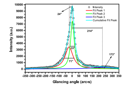
Single crystal and multilayer diffraction (high resolution rocking curves)
Reciprocal space mappings | Orientation matrix
X-ray reflectivity and diffuse scattering from thin film and multilayer structures
In- and out-of-plane grazing incidence diffraction and diffuse scattering.
Monochromatic X-Ray tunable using Double Crystal Monochromator
Energy range
5 KeV-20 KeV
Beam acceptance
1.5 mrad (H) x 0.2 mrad (V)
Focusing optics
Vertical focusing by two cylindrical mirrors and horizontal focusing by sagittal bending of DCM 2nd crystal
Focal spot at sample position
0.30 mm (H) X 0.10 mm (V) at 8 keV
Flux
~109 photons /sec/mm2 at 8 keV
Spectral resolution(Δλ/λ)
1.5x10⁻⁴
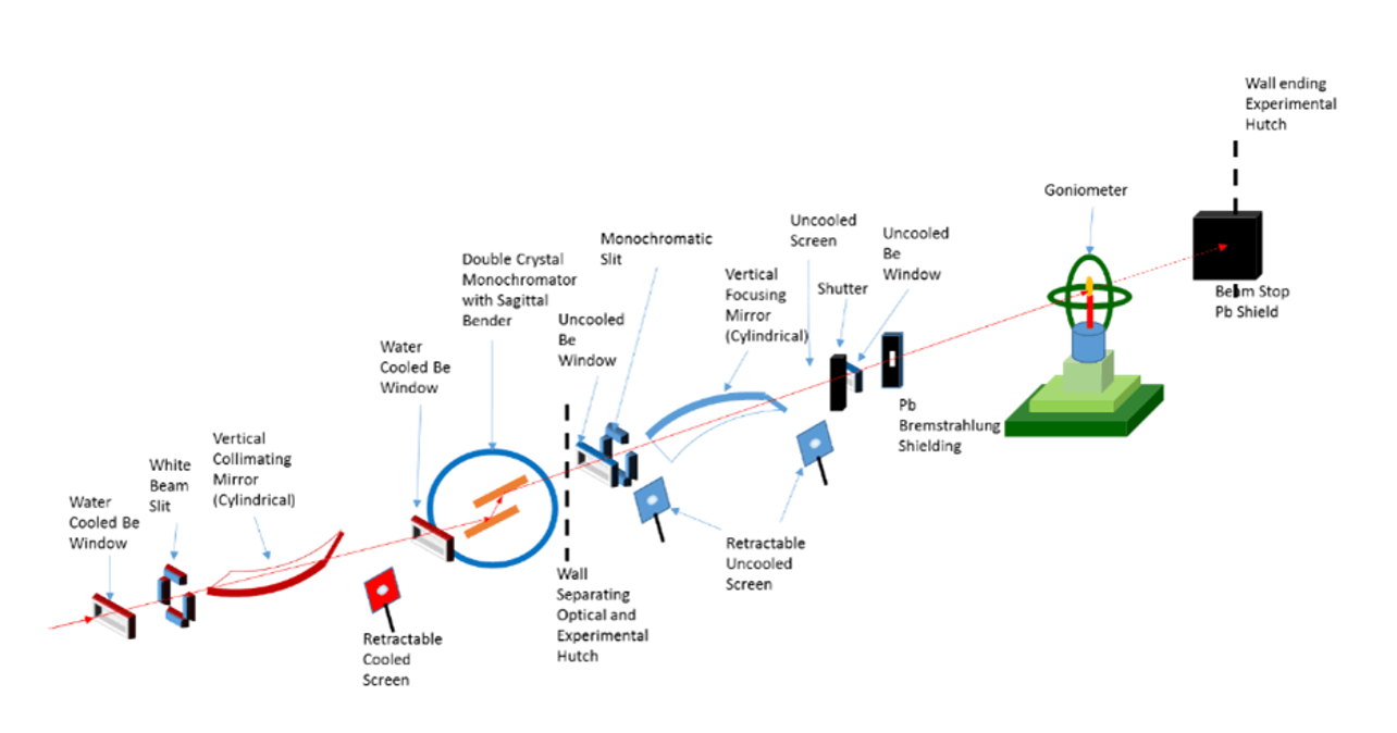
The total length of the beamline, from the tangent point of the storage ring to the sample position, is approximately 32 meters. The front-end of the beam port is connected to the beamline via a water-cooled beryllium (Be) window.
The main optical components of the beamline include:
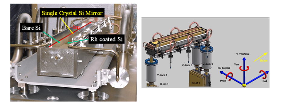
A Vertical Collimating Mirror (VCM)
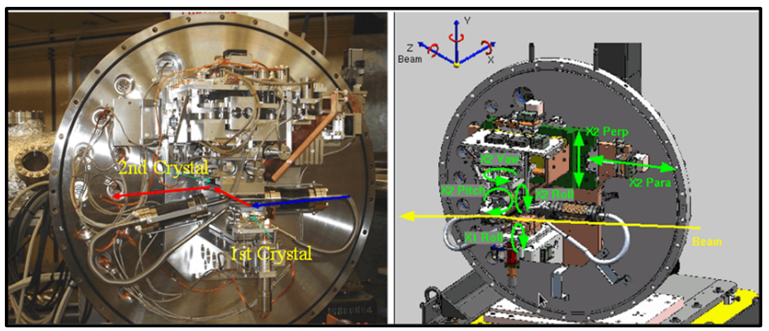
A Double Crystal Monochromator (DCM)
A Vertical Focusing Mirror (VFM)
The two mirrors (VCM and VFM) work together to vertically focus the beam onto the sample or detector position within the diffractometer located in the experimental station. The DCM serves to monochromatize the beam, allowing the transmission of photons in the energy range of 5 keV to 20 keV.
The second crystal of the DCM is bendable, enabling horizontal focusing of the beam at the sample or detector position, as required by the experimental setup.
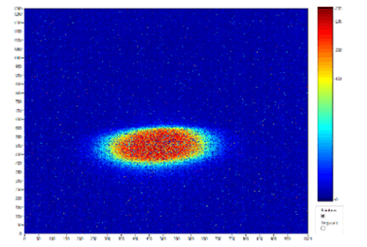
A position monitor named as nano-BPM is placed just before the sample. It is used to image and analyze the beam profile. Additionally, an ion chamber, positioned before the sample, could be used to normalize the incident beam intensity, if needed.
Image of the inside of the DCM and schematics showing different motors of the DCM
Image of the inside of the VCM and schematics showing different motors of the VCM
Nano-BPM image of the focused X-ray beam
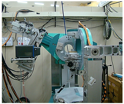
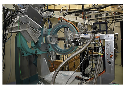
Experimental station
A high-precision Eulerian cradle eight-circle Huber diffractometer, which can accommodate wide variety of sample stages.
Quasi-simultaneous XRD measurements using 2D and 0D detectors
Closed cycle refrigrator for temperature dependent XRD measurement
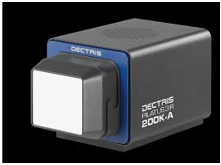
Detectors: 1. 2D Detector:
Pilatus 200k
2.Point detector(s):
Oxford Instruments (C400): Scintillation detector
Radicon: Scintillation detector
Temperature stages:
ARS cryostat (for low temperature XRD measurements)
Heating stages for high temperature measurements
1.
Influence of chemical purification methodologies on the Bridgman growth of trans stilbene (TSB) crystal, and feasibility studies for X ray imaging and neutron/gamma discrimination applications A Pal, S Kar, C Debnath, S R Mohan, R Roychowdhury, A K Agrawal, Sonu, M Tyagi, S Verma
J Mater Sci: Mater Electron 36, 793 (2025)
https://doi.org/10.1007/s10854-025-14845-5
1.
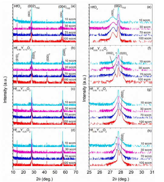
Effect of oxygen partial pressure on phase, local structure and photoluminescence properties of Hf(1-x)YxO2 thin films prepared by pulsed laser deposition M Nand, P Rajput, S Tripathi, M Kumar, Y Kumar, H Bhatt, P Deshmukh, H Srivastava, S K Mandal, R Urkude, S Satapathy, M Gupta, S N Jha
Vacuum, 221, 112882 (2024).
https://doi.org/10.1016/j.vacuum.2023.112882
2.
Effect of oxygen ion implantation on the local electronic structures of strontium titanate single crystals: An investigation using synchrotron-based X-ray diffraction and X-ray photoemission techniques A Kumar, M Baral, A Kandasami, S K Mandal, R Urkude, S Bhunia, V R Singh
J. Appl. Phys., 135, 155302 (2024). https://doi.org/10.1063/5.0202962
3.
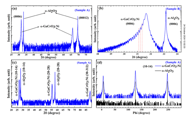
Structural and interface band alignment properties of transparent p-type α GaCrO3: Ni/α – Al2O3 heterojunction 3. R Sharma, K Baraik, H Srivastava, S K Mandal, T Ganguli, R Jangir
J. Appl. Phys., 136, 025304 (2024).
https://doi.org/10.1063/5.0205892
4.
Origin of microscopically coupled ferromagnetic Cu ions in a distorted system of Cu- doped ZnO and their synchrotron based electronic structure A Kumar, T Ghosh, Z Aabdin, J Roy, V K Verma, A Ghosh, S K Sahoo, R Urkude, S Bhunia, U K Goutam, K Amemiya, A Kandasami, V R Singh
AIP advances 14, 025250, (2024).
https://doi.org/10.1063/5.0179935
5.
Local electronic structures of annealing induced phases in Cobalt doped TiO2 nanoparticles: A combined study of transmission electron microscopy and x-ray absorption fine structure spectroscopy R Dawn, R Urkude, S Tripathi, S Bhunia, W W Tjiu, Z Aabdin, A Kandasami, V Raj Singh
Phys. Scr., 99, 045918 (2024).
https://doi.org/10.1088/1402-4896/ad2e56
6.
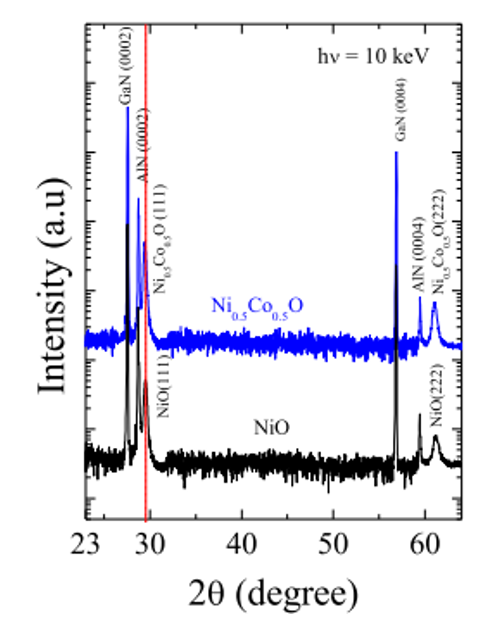
Investigation of crystalline band alignment properties of NiO/GaN and Ni0.5Co0.5O/GaN heterojunctions using Synchrotron radiation-based techniques K Baraik, R Roychowdhury, A Bose, C Mukherjee, T Ganguli, S D Singh
Phys. Scr., 99, 065951 (2024)
https://doi.org/10.1088/1402-4896/ad4524
1.
An Alternative Approach to Study Photo-catalytic Behavior of TiO2 Using Synchrotron-Based Advanced Spectroscopic Techniques A Kumari, M Zaman, A Kumar, V R Singh, A Ghosh, S K Sahoo, A Rahaman, S K Mandal, S Bhunia
J. Mater. Eng. Perform. 32, 10391 – 10401 (2023). https://doi.org/10.1007/s11665-023-07876-8
2.
growth and measurement of photovoltaic properties Md Mohsin, S Bhunia, A. Nayak, Ferroelectric ZnSnS3 thin films
J Mater Sci: Mater Electron. 34, 2194 (2023). https://doi.org/10.1007/s10854-023-11545-w
1.
Different polymorphs of Y doped HfO2 epitaxial thin films: Insights into structural, electronic and optical properties M Nand, S Tripathi, P Rajput, M Kumar, Y Kumar, S K Mandal, R Urkude, M Gupta, A Dawar, S Ojha, S K. Rai, S N Jha
J. Alloys compd., 928, 167099 (2022). https://doi.org/10.1016/j.jallcom.2022.167099
2.
A Technical Report on an Innovative Plan to Migrate from Traditional PCI Card based Control System to USB Port Interfaced Control System that has been Implemented Successfully in an Active Synchrotron Beam Line A Das
J. Eng. Sci. Technol. Rev. 15 (6) 20-27 (2022). https://doi.org/10.25103/jestr.156.03
1.
WS2 Nanosheet/Si p–n Heterojunction Diodes for UV–Visible Broadband Photodetection S Pal, S Mukherjee, R Jangir, M Nand, D Jana, S K Mandal, S Bhunia, C Mukherjee, S N Jha, S K Ray
ACS Appl. Nano Mater., 4, 3241-3251, (2021). https://dx.doi.org/10.1021/acsanm.1c00421
1.
Interface evolution of Cr/Ti multilayer films during continuous to discontinuous transition of Cr layer P Sarkar, A Biswas, S Rai, H Srivastava, S Mandal, M H Modi, D Bhattacharya
Vacuum, 181, 109610 (2020). https://doi.org/10.1016/j.vacuum.2020.109610
Team members
Dr. Dileep Kumar (dkumar[at]csr[dot]res[dot]in) Phone: 0731-2463913 (Extn. 176)
(Scientist)
[Contact for thin films measurements]
Dr. Dinesh Kumar Shukla (dkshukla[at]csr[dot]res[dot]in) Phone: 0731-2463913 (Extn. 239)
(Scientist)
[Contact for powder XRD and single crystal measurements]
Mr. Vinod Savaner (savanervinod[at]gmail[dot]in)
(Scientific Assistant)
Prof. Satyaban Bhunia (satyaban.bhunia[at]saha[dot]ac[dot]in), Phone: 033-2337-5345 (Extn. 3320)
Prof. Mrinimay K. Mukhopadhyay (mrinmay.mukhopadhyay[at]saha[dot]ac[dot]in), Phone: 033-2337- 5345 (Extn. 2521)
Science Highlights
1. Influence of chemical purification methodologies on the Bridgman growth of trans stilbene (TSB) crystal, and feasibility studies for X ray imaging and neutron/gamma discrimination applications
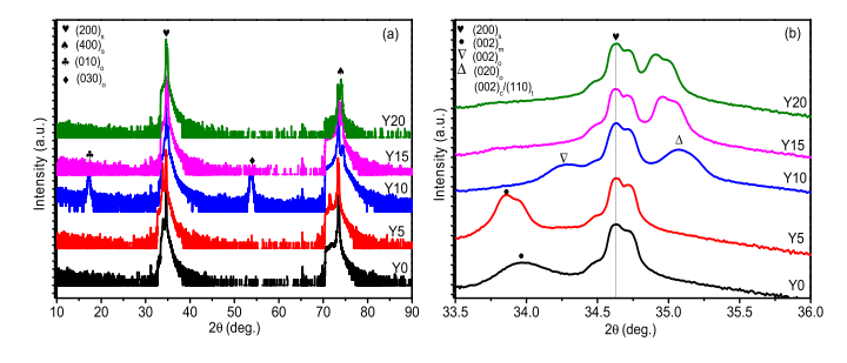
2. Effect of oxygen partial pressure on phase, local structure and photoluminescence properties of Hf(1-x)YxO2 thin films prepared by pulsed laser deposition
3. Effect of oxygen-ion implantation on the local electronic structures of strontium-titanate single crystals: An investigation using synchrotron-based x-ray diffraction and x-ray photoemission techniques
4. Local electronic structures of annealing induced phases in Cobalt doped TiO2 nanoparticles: A combined study of transmission electron microscopy and x-ray absorption fine structure spectroscopy
5. Investigation of crystalline band alignment properties of NiO/GaN and Ni0.5Co0.5O/GaN heterojunctions using Synchrotron radiation-based techniques