This beamline utilizes X-ray diffraction (XRD) technique in energy-dispersive and angle-dispersive modes to carry out experiments mainly focused on engineering problems, viz; stress measurement, texture measurement, micro structure and elastic constants determination in variety of bulk as well as thinfilm samples. The flexible design of beamline allows various types of X-ray scattering experiments such as grazing angle diffraction, X-ray reflectivity and energy dispersive XRD. Additionally, the beamline has insitu high temperature (up to 900 K) facility with vacuum (better than 5×10⁻⁵ mbar) environment. The facility for insitu XRD during mechanical loading will be added soon.
This beamline enables a wide range of experiments:
Residual stress measurements in thinfilms and bulk samples
Powder diffraction, line profile analysis
Energy dispersive XRD
X-ray reflectivity, Resonant X-ray reflectivity
High resolution XRD for epitaxial thin films
High temperature (Room Temperature to ~900 K) and Low Temperature XRD measurements down to ~100 K
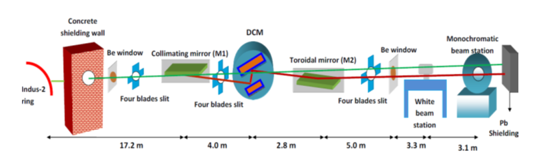
Schematic layout of the engineering application beamline (not to the scale)
Experimental station
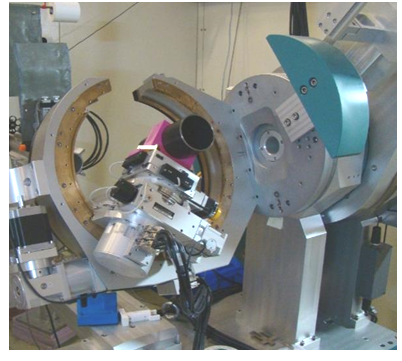
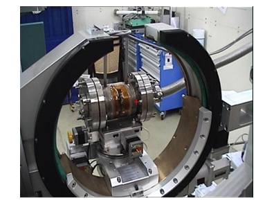
A high-precision open Eulerian cradle six-circle Huber diffractometer :
Can accommodate a sample up to ~15 kg weight, has sphere of confusion of 50 μm for all axis movement.
Can handle a sample size up to: 1000 mm (L), 500 mm (W) and 45 mm thickness.
Allows a high 2θ range up to 170 deg. with a step size accuracy of 0.0002 deg.
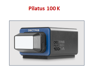
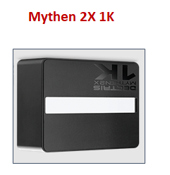
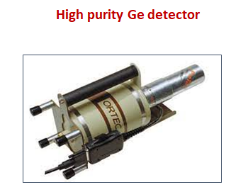
Available Detectors
2D PSD with ~6 deg coverage and pixel size of~0.016 deg
1D PSD with ~3.5 deg coverage and pixel size of ~0.003 deg
Energy range 5 -35 keV
Resolution 122 eV FWHM at 5.9 keV,
Count rates > 1,000,000 CPS
Energy range 5 -300 keV
Resolution 550 eV FWHM at 122 keV,
Count rates > 50,000 CPS
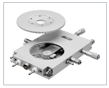
Heating-cooling stages
A high temperature stage (reflection geometry) for insitu XRD experiments from RT to ~900 K under high vacuum atmosphere (better than 5×10⁻⁵ mbar) , temperature stability ~0.5 K and 2θ range up to 100 deg.
Linkam stage (transmission geometry)
temperature range from 77 K to 873 K
high heating rate upto 150 K/min
2θ range of ~40 deg.
1.
Synchrotron XRD for Residual Stress Measurement in Multipass Narrow Gap Dissimilar weld of P92 and SS304 Steel Meena, P., Anant
R. Trans Indian Inst Met 79, 12 (2026).
2.
Microstructure analysis of low electron density contrast metallic multilayers using resonant X‐ray reflectivity P. N. Rao,M. K. Swami, H. Srivastava,,P. Sahu,, A. Ghosh and S. K. Rai,
J. Synchrotron Rad. 33, 708–714 (2026).
1.
Studies on the proximity effect in Bi-based high temperature superconductor/manganite heterostructures Gayathri V., E. P. Amaladas, A. T. Sathyanarayana, T. Geetha Kumary, R. Pandian, Pooja Gupta, Sanjay K. Rai and Awadhesh Mani
Phys. Chem. Chem. Phys., ,27, 9607-9619 (2025).
2.
Unravelling the subgrain stabilities of microstructures across P91 steel weld joint under creep-fatigue interaction loading waveforms through EBSD and synchrotron based XRD studies P. Vaishali, Vani Shankar, Ashok Bhakar, Sanjay Rai,, Materials Characterization
Volume 224,115062 (2025).
3.
Controlled Surface Rolling: A Novel Low Plasticity Burnishing Technique to Mitigate Stress Corrosion Cracking in Machined SS304L Saradhi Gumma, M. K. Swami, G. Bharat Reddy, P. Ganesh, H. Donthula, Sanjay Kumar Rai & Supratik Roychowdhury
J. of Materi Eng and Perform 34, 11101(2025).
4.
Structure, stress, and optical property correlations in nano-structured Mo/Si and W/B4C multilayer mirrors for hard x-ray applications F. Mollick, M. Nayak, A. K. Kashyap, J. Kumar, A. Majhi, N. Pothana, P. Rajput, M. K. Tiwari, S. K. Rai, M. N. Singh & A. Sagdeo
J. Appl. Phys. 138, 175303 (2025).
5.
Deciphering the role of Nb driven interface engineering on the magneto-structural properties of W/CoFeB Heterostructures Neha Gupta, Harsh Bhatt, Anirudhha Bose Mukul Gupta, Surendra Singh, S.K. Rai, Pooja Gupta
Journal of Alloys and Compounds,1035, 181571 (2025).
6.
Effect of Al doping on structural, electronic, mechanical, and optical properties of VN thin films. A. K. Verma, R. Gupta, Pooja Gupta, S. Rai, S. Prakash, A. Tayal, A. Gloskovskii, R. Ramaseshan, P. Garg, U. Deshpande & M. Gupta
Applied Surface Science Advances 30, 100884 (2025).
7.
Studies on magnetron sputtered niobium thin films: influence of deposition angle of sputtered atoms P. N. Rao, M. K. Swami, Amrit Ghosh, R. Jangir & S. K. Rai
Appl. Phys. A 131, 168 (2025).
8.
Exploring Oxygen Vacancies in Sputtered HfO2 Films for Multi-Bit RRAM Applications Tanmayee Parida, Sonali Patajoshi, Bisweswar Santra, Ummiya Qamar, Aniruddha Bose, P. N. Rao, Sanjay Rai, Santanu Das, Aloke Kanjilal
Adv. Mater. Technol.10, no. 22, e00289 (2025).
9.
Glancing Angle Deposition-Induced Asymmetric Growth and Magnetic Anisotropy in Co2FeAl/C60 Thin Films Sonia Kaushik, Rakhul Raj, Manisha Priyadarsini, Pooja Gupta, Gouranga Manna, Varimalla Raghavendra Reddy, and Dileep Kumar
ACS Applied Electronic Materials,7, 3000 (2025).
10.
Growth-induced magnetic anisotropy in Co/C60 bilayers: Insights from a two-grain Stoner-Wohlfarth model Sonia Kaushik ,Rakhul Raj , Pooja Gupta ,Andrei Chumakov, Matthias Schwartzkopf ,V. Raghavendra Reddy and Dileep Kumar
Phys. Rev. B 111, 184426 (2025).
11.
Effect of TIG-arcing speed on the microstructure vis-`a-vis mechanicalbehaviour of surface modified low carbon steel Sachin Balbande, Sanjay Rai, Gautam Agarwal, Sourav Das
Wear, 570, 2059241 (2025).
12.
Structural changes in amorphous Co40Fe40B20 thin film interfaced with tungsten upon thermal annealing: A depth resolved XRD and XAS study Mandeep Singh, Pooja Gupta, Sanjay Rai, Sarathlal Koyiloth Vayalil, Mukul Gupta, Ilaria Carlomagno, Carlo Meneghini, Ajay Gupta
Surfaces and Interfaces, 56, 105716 (2025).
13.
Does compaction pressure control densification, dislocation density and texture evolution in spark plasma sintered WC. An investigation by SXRD and EBSD Arun Kumar Panda, R. Mythili, R. Thirumurugesan, Pradyumna Kumar Parida, T. Sreepriya, S. K. Rai & Arup Dasgupta
Philosophical Magazine, 1, (2025).
14.
Residual stress mitigation in dissimilar T/P92 and AISI304L steel multi-pass weld joint using ER308L and ERNiCrMo-3 (IN625) fillers: simulation and experimental approach, Meena, P., Anant, R.,
Weld World (2025).
1.
Improvement of Stress Corrosion Cracking Resistance of Shear Cut 304L Stainless Steel through Laser Shock Peening R.K. Gupta, A.K. Rai, D.C. Nagpure, R. Biswal, P. Ganesh, S.K. Rai, K. Ranganathan, K.S. Bindra, and R. Kaul
J. of Materi Eng and Perform 33, 8983–8993 (2024).
2.
Effect of deformation mode on martensitic transformation in medium Mn steel Poornachandra Satyampet, Subhas Bhunia, Saurabh Kundu, Prita Pant
Materialia,34, 102065 (2024).
3.
Investigations on structure and optical properties of neutron irradiated nanocrystalline La2Zr2O7 pyrochlores Tanmoy Biswas, Sujoy Sen, K. Chitrarasu, Pooja Gupta, P. Thangadurai, S. Amirthapandian
Radiation Physics and Chemistry,223, 111949 (2024).
4.
Quantitative analysis of deformation characteristics and corrosion properties of high energy laser shock peened Ni-based superalloy Yarramilli Vamsi Apuroop, Sanjay Rai, Malar Vadani, Sabeur Msolli, Pooja Gupta, Sanjay Rai, Niroj Maharjan, Ayan Bhowmik
Surface and Coatings Technology, Volume 494, 131470 (2024).
1.
Evading the strength-ductility compromise in medium manganese steel by a novel low temperature warm rolling treatment A. Chandan, G. Mishra, K. Kishore, G. Bansal, B. Sahoo, P. Jena, S. Kumar, S. Rai, R. Saha, S. Kundu & J. Chakraborty
Mater.Charact. 206, 113445(2023) https://doi.org/10.1016/j.matchar.2023.113445
2.
Anisotropic magnetic and magnetotransport properties in morphologically distinct Nd0. 6Sr0. 4MnO3 thin films RS Mrinaleni, EP Amaladass, AT Sathyanarayana, S Amirthapandian, J. P, Pooja Gupta, T. Geetha Kumary, S. K. Rai & A. Mani
Physica Scripta 98 (7), 075919 (2023) https://doi.org/10.1088/1402-4896/acd733
3.
Interfacial interaction driven enhancement in the colossal magnetoresistance property of ultra-thin heterostructure of Pr0.6Sr0.4MnO3 in proximity with Pr0.5Ca0.5MnO3 V. Gayathri, E. P. Amaladass, A. T. Sathyanarayana, T. Geetha Kumary, R. Pandian, Pooja Gupta, S. K. Rai & A. Mani
Scientific Reports 13, 2315 (2023)
https://doi.org/10.1038/s41598-023-28314-8
4.
Enhanced temperature coefficient of resistance in nanostructured Nd0.6Sr0.4MnO3 thin films. M. R S, E. P. Amaladass, S. Amirthapandian, A. Sathyanarayana, J. P, K. Ganesan, C. Ghosh, R. M. Sarguna, P. Rao, Pooja Gupta, T. G. Kumary, A. Dasgupta, S. Rai & A. Mani
Thin Solid Films, 779, 139933 (2023)
https://doi.org/10.1016/j.tsf.2023.139933
5.
Study of oxidation behaviour of Ruthenium thin film after thermal annealing in oxygen environment S. Gupta, M. Sinha, R. Dhawan, R. Jangir, A. Bose, Pooja Gupta, M. Swami & M. H. Modi
Thin Solid Films, 764, 139606 (2023)
https://doi.org/10.1016/j.tsf.2022.139606
6.
Effect of Chemo-mechanical Polishing on the Surface and Superconducting Properties of Niobium Coupons: A Comparative Study J Chandra, PN Rao, S Rai, M Manekar
Journal of Superconductivity and Novel Magnetism 36 (3),777-791 (2023).
https://doi.org/10.1007/s10948-023-06499-3
1.
Structural characterization of Au/Cr bilayer thin films using combined X‐ray reflectivity and grazing incidence X‐ray fluorescence measurements M. A. Alam, M. K. Tiwari, A. Khooha, M. Nayak & C. Mukherjee
Surf. Interface Anal. 54, 1032 (2022)https://doi.org/10.1002/sia.7128
1.
BL-02: a versatile X-ray scattering and diffraction beamline for engineering applications at Indus-2 synchrotron source Pooja Gupta, PN Rao, MK Swami, A Bhakar, Sohan Lal, SR Garg, CK Garg, PK Gauttam, SR Kane, VK Raghuwanshi, SK Rai,
Journal of Synchrotron Radiation 28 (4), 1193-1201, 2021
2.
Line profile analysis of synchrotron X-ray diffraction data of iron powder with bimodal microstructural profile parameters A Bhakar, P Gupta, PN Rao, MK Swami, P Tiwari, T Ganguli, SK Rai ,
Journal of Applied Crystallography 54 (2), 498-512, 2021
Team members
Dr. S.K. Rai (sanjayrai[at]rrcat[dot]gov[dot]in)
Dr. Mahesh Kumar Swami
Dr. Pooja Gupta
Dr. Nageswrarao Pothanna
Mr. Ashok Bhakar
Science Highlights
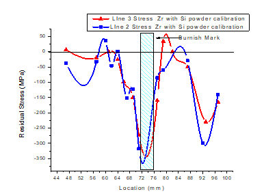
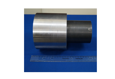
1. Residual stress measurement on inside wall of roll bonded Zircaloy SS pressure tubes used in PHWRs. These samples had diameter of 150 mm, length 200 mm and weight of 12 kg.
Stress profile on the inside surface
Photograph of the sample
This work was done in collaboration with RED, BARC.
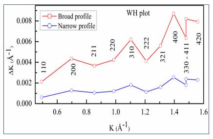
2. Microstructure assessment of Fe powder using line profile analysis
The super-Lorentzian peak shapes of XRD data of Fe were modeled using convolution of bimodal microstructural parameters. The dislocation densities estimated for narrow and broad profile were about 2×10¹⁴ and 2×10¹⁵ m-2.
Profile fitting of a 200 Bragg peak using convolution of bimodal microstructure.
Comparison of deconvoluted narrow and broad profiles of Bragg peaks of Fe powder using WH plot.
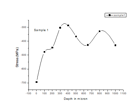
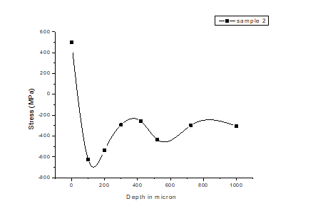
3. Depth dependent stress profile on laser shock peened Ni based super-alloys for aerospace applications
Stress profile on sample peened with tape
Stress profile on sample peened without tape
Depth profiling was done by sequential electro-polishing on the alloy samples. These results were matched well with FEM simulations. This work was done in collaboration with Materials Science Engineering department of IIT Delhi.