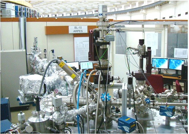
Angle resolved photoelectron spectroscopy (ARPES) is an experimental technique that is widely used to study the occupied electron density of states, and the mapping of valence band structure of solid-state materials. The ARPES beamline (BL-10), which has been commissioned in March 2021, is designed to use the photon energy in the range from 30 eV to 1,000 eV, with a planer undulator as its source. The synchrotron beam is monochromatized using variable line spacing plane grating (VLS-PG) based monochromator. The photoemission experimental station consists of dedicated preparation and analysis chambers. The preparation chamber is equipped with LEED and sample cleaning facilities such as sputtering, annealing (e-beam heating), scraping and cleaving. The analysis chamber is equipped with a 5-axis manipulator, closed cycle refrigerator (CCR), hemispherical electron energy analyser and flood gun. Experiments can be carried out at low temperature down to ~20 K. The beamline is optimised to carryout angle resolved photoelectron spectroscopy measurements, valence band spectroscopy in the angle integrated mode, resonant photoelectron spectroscopy, etc.
The Photograph of Beamline
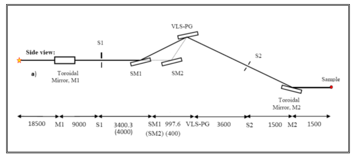
Beamline parameters & Optical layout
The ARPES beamline (BL-10) uses a plane polarized light emitted by a planar undulator, U2.
Planar undulator parameters
Energy Range
30 eV to 1000 eV
Periodic Length
85.2 mm
Peak Magnetic Field
0.86 Tesla
K values
6.83 to 1.6
Number of Periods
24
Beamline Parameters
Energy Range
30 eV – 1000 eV
Resolution
35 meV at 90 eV photon energy
Flux (calculated)
5×10¹¹ photons/sec/200 mA
Beam Size
300 µm (H) × 100 µm (V) approximately
Monochromator
Four VLS –Plane Gratings
Optical layout of the beamline
First optical element is a vertically mounted toroidal mirror, M1, which accepts the central cone of ID beam emitted within 1 mrad (H) × 0.4 mrad (V) divergence.
The M1 focuses the beam vertically on the entrance slit, and horizontally in front of monochromator.
Monochromator is consists of four VLS-PGs (290 l/mm, 770 l/mm, 700 l/mm and 1400 l/mm) and two spherical mirrors(SMs), and is operated in constant included angle mode or Monk-Gillieson configuration.
Two SMs provided two different included angles to cover the wide energy range and to reduce the thermal load from undulator on the grating by operating the monochromator in lower and higher energy mode.
The last optical element is a horizontally mounted toroidal mirror, M2, which focuses the beam on the sample within the spot size of 300 µm (H) × 100 µm (V).
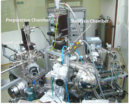
Experimental station
The experimental station of the beamline comprises of a load lock chamber, a preparation chamber and an analysis chamber. The samples can be transferred between the chambers without breaking vacuum.
Analysis chamber
Material of construction
Mu metal
Base vacuum
7x10-11 mbar
Electron analyser
Phoibos 150 HSA
Energy resolution: 2 meV
Angular resolution: 0.1°
Flood gun
Upto 10 eV for insulating samples
Sample manipulator
5 axis with sample cooling with CCR down to 20 K
Preparation chamber
Base pressure of preparation chamber
5x10-11 mbar
In-situ sample preparation
Ar ion sputtering
Cleaving
Scrapping
Sample heating
Upto 800 K
LEED system
Present
The experimental station also has a monochromatized He sources (21.2 eV and 40.8 eV), non-monochromatized twin anode X-ray sources (Al Kα: 1486.5 eV and Mg Kα: 1253.6 eV). Before the commissioning of the beamline in March 2021, these sources were in use for several experiments.
Application Areas
Surface Science
Separate bulk and surface sensitive information by tuning the photon energies.
Chemistry
Surface composition, surface modification by in-situ sputtering and annealing.
Phase transition
Temperature dependent measurements to determine the electronic structure across the crystallographic or magnetic phase transitions.
Applied research
Analysis and expertise of various applied problems in surface science.
Basic research
Determination of density of states, band structure and Fermi surface mapping of novel materials.
1.
Effect of laser fluence on signal sustainability and quantitative performance of fiber-optic LIBS for steel samples.
Sunita Ahlawat, Diksha Garg, Priya Tripathi, Rajesh Kumar Sahu, Soma Banik, Pravin S. Hedaoo, B. Prasad, Rashmi Singh, P.K. Mukhopadhyay, B.N. Upadhyaya.
Spectrochimica Acta Part B: Atomic Spectroscopy 235, 107362 (2026).DOI: 10.1016/j.sab.2025.107362.
2.
Engineering Al-doped ZnO/PDMS flexible triboelectric nanogenerators through SiO2 interlayer and MoS2 nanofillers for enhanced performance
Abhinav Mahapatra, R. S. Ajimsha, Rajiv Kamparath, Kritika Vijay, D. Deepak, Soma Banik, C. Mukherjee, Susanta Sinha Roy, Sunil Verma and Pankaj Misra.
Journal of Material Chemistry A, 14, 4490 (2026).DOI: 10.1039/d5ta08337k.
3.
Electron Doping in Single-Crystalline BaBiO3: BaBiO3−xFx
Sathishkumar M, Asha Ann Abraham, Rajesh Kumar Sahu, Manisha Srivastava, Soma Banik, Soham Manni
Physica Status Solidi A, 223, e202500600(1-5) (2026),DOI: 10.1002/pssa.202500600.
4.
Coupled influence of infiltration temperature of sulfur and carbonate electrolyte on Li–S battery performance.
Manisha Patro, Nadeema Ayasha, Jay Soni, Rajesh Kumar Sahu, Soma Banik, Sagar Mitra
Journal of Energy Storage 156, 121590 (2026).DOI: 10.1016/j.est.2026.121590.
5.
Localized RF Heating-Driven Thermoelectric Power Generation in Natural Galena (PbS).
Karthik R, Yiwen Zheng, Rajesh Kumar Sahu, Sreeram Punathil Raman, Soma Banik, Aniruddh Vashisth, and Chandra Sekhar Tiwary
ACS Applied Electronic Material 8, 1600−1613 (2026).DOI: 10.1021/acsaelm.5c02240.
6.
Structural, optical, and electronic structure properties of Cu substituted NiO solid solutions.
Kiran Baraik, Velaga Srihari, Rajashri R. Urkude, Pragya Tiwari, Mukul Gupta, R. J. Choudhary, Chandrachur Mukherjee, Biplab Ghosh, Tapas Ganguli, Shreyashkar Dev Singh.
Journal of Applied Physics 139, 165706 (2026).DOI: 10.1063/5.0325289.
7.
Surface transfer n-type doping of graphene using WO3 nanoparticles prepared without the use of hazardous chemicals
Visheshvar Verma, Avinash Mahapatra, Rajesh Kumar Sahu, Ram Sevak Singh, Atikur Rahman, Mukul Gupta, Soma Banik and Arun Kumar Singh
Journal of Material Chemistry C (2026). DDOI: 10.1039/d6tc00248j.
8.
Tuning VO2 phase stability by Cr doping: insights from photoemission and X-ray absorption spectroscopic investigations
Riya Dawn, Madhusmita Baral, Rajashri Urkude, Luo Ping, Zainul Aabdin, Biplab Ghosh and
Vijay Raj Singh
Journal of Materials Chemistry C 2026.DOI: 10.1039/d5tc04234h.
1)
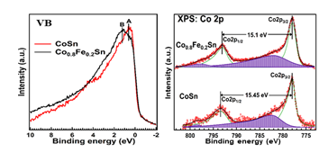
Effect of Fe doping on the electronic properties of CoSn Kagome semimetal.
Kritika Vijay, Kawsar Ali, Najnin Bano, Anju Ahlawat, Mukul Gupta, Ram Janay Choudhary, D K Shukla, Ashok Arya, Soma Banik.
Journal of Physics: Condensed Matter, 37, 095502 (2025).DOI: 10.1088/1361-648X/ad9a46.
2)
Competing Magnetic Interactions in the Antiferromagnetic Kagome Semimetal Fe1-yCoySn.
Kritika Vijay, K. Kumar, Soma Banik.
Journal of Superconductivity and Novel Magnetism 38, 106 (1-6) (2025).DOI: 10.1007/s10948-025-06943-6
3)
Valence fluctuations in Co-doped FeSn antiferromagnetic kagome semimetal.
Kritika Vijay, Rajeev Joshi, Kranti Kumar, Sudip Nath, and Soma Banik.
Journal of Applied Physics 137, 205104 (2025).DOI: 10.1063/5.0253820
4)
Metal-insulator transition in FeSex originating in an anomalous lattice effect.
Shubham Purwar , Shinjini Paul , Kritika Vijay , R. Venkatesh , Soma Banik, P. Mahadevan , and S. Thirupathaiah.
Physical Review B 111, 085123 (2025).DOI: 10.1103/PhysRevB.111.085123
5)
Mitigating parasitic contributions in measured piezoresponse for accurate determination of piezoelectric coefficients in Sc-alloyed-AlN thin films using piezoresponse force microscopy
Ch Kishan Singh, Rajalakshmi K, Balamurugan N, Rakesh Kumar, Mukul Gupta, Ramaseshan R, and Kiran Baraik
Journal of Applied Physics 138, 075302 (2025).DOI: 10.1063/5.0281407
6)
Structural and interface band alignment investigations on epitaxial β-Ga2O3/α-GaCrO3 type-II transparent heterojunction.
Rishav Sharma, Prabhat Kumar Singh, Kiran Baraik, Himanshu Srivastava, Satish Kumar Mandal, Nageswararao Pothana, Salahuddin Khan, Rupesh S. Devan, Tapas Ganguli, Ravindra Jangir.
Journal of Applied Physics 138, 065301 (2025).DOI: 0.1063/5.0284059
7)
Identification of Surface, Interface, and Bulk States on the Pristine and Passivated InP (001) and (111) Surfaces Using Surface Photovoltage Spectroscopy
Deepesh Nimje, Geetanjali Vashisht, Venus, Sanjay Porwal, Soma Banik, Pooja Gupta, Tarun Kumar Sharma, and Vijay Kumar Dixit
Physica Status Solidi RRL 1, 2500226 (2025)DOI: 10.1002/pssr.202500226 .
8)
Orbital Angular Momentum-Driven Ferromagnetism with Magnetic Anisotropy and Electronic Structure of Epitaxial Neodymium Nitride
Renuka Karanje, Anupam Bera, Sourav Rudra, Debmalya Mukhopadhyay, Souvik Banerjee,
Manisha Bansal, Kiran Baraik, Sourav Chowdhury, Weibin Li, Manuel Valvidares, Tuhin Maity, and Bivas Saha.
ACS Nano 19, 36636−36645 (2025).DOI: 10.1021/acsnano.5c11890 .
9)
Carbon ion implantation for electron compensation in epitaxial scandium nitride.
Sourav Rudra , Dheemahi Rao, Sneha Kobri M, Aritra Dey, Renuka Karanje, Prasanna Das, Subhajit Manna, Madhusmita Baral, Bhupesh Yadav, Ashalatha Indiradevi Kamalasanan Pillai, Magnus Garbrecht, Mukul Gupta, Satyaprakash Sahoo, Tapas Ganguli, and Bivas Saha.
Physical Review B 112, 165302 (2025).DOI: 10.1103/b5x8-c1bl .
10)
A Combined Theoretical and Experimental Investigation on an Fe Doped Bi2Se3 Topological Insulator.
Ravi Kumar, D. S. Sisodiya, Kritika Vijay, Soma Banik, Shashwati Sen, P. D. Babu,
and Dibyendu Bhattacharyya
Journal of Physical Chemistry C 129, 19514 (2025).DOI: 10.1021/acs.jpcc.5c03940.
11)
Co doped Bi2Se3 topological insulator: a combined theoretical and experimental study.
Ravi Kumar, D. S. Sisodiya, Kritika Vijay, Soma Banik, Shashwati Sen, P. D. Babu, and Dibyendu Bhattacharyya.
Materials Science in Semiconductor Processing 195, 109572 (2025).DOI:10.1016/j.mssp.2025.109572.
Photoemission spectroscopy and ab-initio simulation of CrFeVGa and CoFeVSb: a comparative study.
J. Nag, Kritika Vijay, B. Bandyopadhyay, Soma Banik, A. Alam, K. G. Suresh.
Journal of Physics: Condensed Matter 37, 155901 (2025).DOI: 10.1088/1361-648X/adb925.
14)
Tuning output of ZnO piezoelectric nanogenerators through V-doping and SiO2 interlayer
Abhinav Mahapatra, R.S. Ajimsha, Kritika Vijay, Rajiv Kamparath, Manami Midday, Soma Banik, C. Mukherjee, Sunil Verma, Pankaj Misra.
Emergent Materials 8, 8223 (2025). DOI: 10.1007/s42247-025-01259-6 .
1.
Electronic correlation driven magnetic interactions in Fe1−yCoySn kagome semimetal. Kritika Vijay, Kawsar Ali, Kranti Kumar, Archna Sagdeo, Ashok Arya, and Soma Banik.
Physical Review B, 110, 085163 (2024). DOI: 10.1103/PhysRevB.110.085163
2.
Resonant photoemission studies on Fe-Ni alloys.
Ananya Sahoo, V.R.R. Medicherla, Kritika Vijay, Soma Banik.
Journal of Alloys and Compounds, 994, 174544 (2024). DOI: 10.1016/j.jallcom.2024.174544
3.
Investigation of crystalline and band alignment properties of NiO/GaN and Ni0.5Co0.5O/GaN heterojunctions using synchrotron radiation based techniques. Kiran Baraik, Rijul Roychowdhury, Aniruddha Bose, Chandrachur Mukherjee, Tapas Ganguli and S D Singh.
Physica Scripta, 99, 065951 (2024). DOI: 10.1088/1402-4896/ad4524
4.
Strain-induced valence band splitting enabling above-bandgap exciton luminescence in epitaxial Mg3N2 thin films. Nidhi Shukla, Sourav Rudra, Renuka Karanje, Debmalya Mukhopadhyay, Prasanna Das, Bidesh Biswas, Madhusmita Baral, Mukul Gupta, and Bivas Saha.
Chemistry of Materials, 36, 5563 (2024). DOI: 10.1021/acs.chemmater.4c00524
5.
Effect of oxygen-ion implantation on the local electronic structures of strontium-titanate single crystals: An investigation using synchrotron-based x-ray diffraction and x-ray photoemission techniques. A. Kumar, M. Baral, A. Kandasami, S. K. Mandal, R. Urkude, S. Bhunia, and V. R. Singh.
Journal of Applied Physics, 135, 155302 (2024). DOI: 10.1063/5.0202962
6.
Small polaron hopping and tunneling transport in Maxwell–Wagner relaxation dominated Al2O3/TiO2 subnanometric laminates. Partha Sarathi Padhi, S. K. Rai, Kritika Vijay, Himanshu Srivastava, Soma Banik,R. S. Ajimsha, A. K. Srivastava, and Pankaj Misra.
Applied Physics Letters, 124, 233504 (2024). DOI: 10.1063/5.0202776
7.
Tunable Nanobattery Effect and Negative Differential Resistance Characteristics in Interfacial Polarization-Dominated Al2O3/TiO2 Nanolaminates. Partha Sarathi Padhi, Sanjay K. Rai, Kritika Vijay, Himanshu Srivastava, R. S. Ajimsha, Soma Banik, Arvind K. Srivastava, and Pankaj Misra
ACS Applied Nano Materials, 7, 13928 (2024). DOI: 10.1021/acsanm.4c02024
1.
Magneto-strain effects in 2D ferromagnetic van der Waal material CrGeTe3. Kritika Vijay, Durga Sankar Vavilapalli, Ashok Arya, S. K. Srivastava, Rashmi Singh, Archna Sagdeo, S. N. Jha, Kranti Kumar and Soma Banik.
Scientific Reports, 13, 8579 (2023). DOI: 10.1038/s41598-023-35038-2
2.
Tunable magnetoresistance driven by electronic structure in Kagome semimetal
Co1-xFexSn.
Kritika Vijay, L. S. Sharath Chandra, Kawsar Ali, Archna Sagdeo, Pragya Tiwari, M. K. Chattopadhyay, A. Arya and Soma Banik.
Applied Physics Letters, 122, 233103 (2023). DOI: 10.1063/5.0153865
3.
Large unsaturated magnetoresistance and electronic structure studies of single-crystal GdBi Gourav Dwari, Souvik Sasmal, Shovan Dan, Bishal Maity, Vikas Saini, Ruta Kulkarni, Soma Banik, Rahul Verma, Bahadur Singh, and Arumugam Thamizhavel.
Physical Review B, 107, 235117 (2023). DOI: 10.1103/PhysRevB.107.235117
4.
Multiple magnetic phases and anomalous Hall effect in Sb1.9Fe0.1Te2.85S0.15 topological insulators. Debarati Pal, Abhineet Verma, Mohd Alam, Sambhab Dan, Amit Kumar, Seikh Mohammad Yusuf, Soma Banik, Sujay Chakravarty, Satyen Saha, Swapnil Patil, and Sandip Chatterjee.
Journal of Physical Chemistry C, 127, 2508 (2023). DOI: 10.1021/acs.jpcc.2c06655
5.
Nonmagnetic Sn doping effect on the electronic and magnetic properties of antiferromagnetic topological insulator MnBi2Te4. Susmita Changdar, Susanta Ghosh, Kritika Vijay, Indrani Kar, Sayan Routh, P.K. Maheshwari, Soumya Ghorai, Soma Banik, S. Thirupathaiah.
Physica B, 657, 414799 (2023). DOI: 10.1016/j.physb.2023.414799
6.
Ultrafast carrier relaxation and second harmonic generation in a higher-fold Weyl Fermionic system PtAl. Vikas Saini, Ajinkya Punjal, Utkarsh Kumar Pandey, Ruturaj Vikrant Puranik,Vikash Sharma, Vivek Dwij, Kritika Vijay, Ruta Kulkarni, Soma Banik, Aditya Dharmadhikari, Bahadur Singh, Shriganesh Prabhu, and A. Thamizhavel.
Advanced Physics Research, 3, 2300063 (2023). DOI: 10.1002/apxr.202300063
1.
Spin reorientation transition driven by polaronic states in Nd2CuO4. Soma Banik, Kritika Vijay, Suvankar Paul, Najnin Mansuri, D. K. Shukla, S. K. Srivastava, Archna Sagdeo, Kranti Kumar, Shilpa Tripathi and S. N. Jha.
Materials Advances, 3, 7559 (2022). DOI: 10.1039/d2ma00314g
2.
Theoretical and experimental investigations on Mn doped Bi2Se3 topological insulator. Ravi Kumar, Soma Banik, Shashwati Sen, Shambhu Nath Jha , and Dibyendu Bhattacharyya.
Physical Review Materials, 6, 114201 (2022). DOI:10.1103/PhysRevMaterials.6.114201
3.
Blocking Si-induced visible photoresponse in n-MgxZn1–xO/p-Si heterojunction UV photodetectors using MgO barrier layer. Shantanu K. Chetia, Amit K. Das, Rohini S. Ajimsha, Soma Banik, Rashmi Singh, Partha S. Padhi, Tarun K. Sharma, and Pankaj Misra
Physica Status Solidi A, 219, 2200285 (2022). DOI: 10.1002/pssa.202200285
4.
Revealing the impact of prestructural ordering in GaSb thin films. Joshua Asirvatham, Minh Anh Luong, Kiran Baraik, Tapas Ganguli, Alain Claverie, and Aloke Kanjilal.
Journal of Physical Chemistry C, 126, 15405 (2022). DOI: 10.1021/acs.jpcc.2c02893
1.
Influence of Fe doping on the electronic structure of Kagome semimetal CoSn. Kritika Vijay, Archna Sagdeo, Pragya Tiwari, Mukul Gupta and Soma Banik.
Manuscript submitted to DAE-Solid State Physics Symposium 2021
2.
Effect of Mn doping in Bi2Se3 topological insulator: probed by DFT and ARPES. R. Kumar, Soma Banik, Shashwati Sen, A.K. Yadavand D. Bhattacharyya,
Manuscript submitted to DAE-Solid State Physics Symposium 2021
Science Highlights
Influence of Fe doping on the electronic structure of Kagome semimetal CoSn.
Fe doping in CoSn found to increase the valence band (VB) width and decreases the Co 2p spin-orbit coupling which indicates the strong hybridization between the Fe and Co valence states.
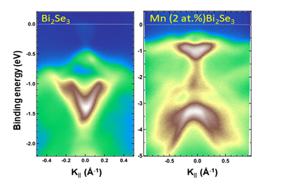
Effect of Mn doping in Bi2Se3 topological insulator: probed by DFT and ARPES.
ARPES studies showed that the magnetic ion doping in the topological insulator Bi2Se3 not only opens up the energy gap in surface states but also changes the bulk band structure significantly.