Quantum Structures of ZnO
A semiconductor structure having at least one dimension comparable to wavelength of electrons and holes is defined as a semiconductor quantum structures. These quantum structure show size dependent properties different from those of a macroscopic semiconductor for example the optical and transport properties that are quite different from the crystalline bulk matter. Among other semiconductors, the current spurt of research in ZnO quantum structures is driven by an almost visible possibility of developing ZnO based low cost and energy efficient UV-blue and white light emitting devices and transparent logics.
1. ZnO/MgxZn1-xO multiple quantum wells
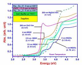
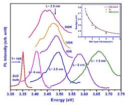
We have studied temperature dependent photoluminescence (PL) from ZnO Multiple Quantum Wells (MQWs) with active layer thickness in the range of ~ 1 - 4 nm grown on (0001) Sapphire by pulsed laser deposition using an in-house developed buffer assisted growth scheme. To the best of our knowledge we have observed for the first time an efficient room temperature PL emanating from such MQWs. In the range of 10K to room temperature (RT), the spectral position of the PL peak shifted monotonically towards red with the increasing temperature in accordance with the empirical Varshni’s relation due to the band-gap shrinkage. The spectral line width was found to increase with increasing temperature due to the scattering of excitons with acoustic and optical phonons in different temperature regimes. At 10K the PL peak shifted from ~ 3.4 to ~ 3.7 eV with decreasing thickness of the quantum well active layer from ~ 4 to 1 nm in good agreement with the calculated quantum confinement effects. From the observations of excitonic features at RT entwined with the band-edge in the absorption spectra of these MQWs these PL transitions are expected to be excitonic in nature and hence highly efficient.
2. Multilayered stacks of ZnO quantum dots
Although a significant wisdom on ZnO based quantum wells is created and reported in the literature the work on ZnO Quantum Dots (QDs) grown on solid substrates is quite scanty. A study on ZnO QDs grown on solid substrate is important not only to understand the three dimensional quantum confinement effects on the excitonic transitions but also to create new forms of this material which could open more frontiers for its applications. As an example, by growing QDs one can enhance the linear and nonlinear responses in ZnO significantly. To the best of our knowledge we have grown for the first time, multilayer of ZnO QDs of varying size by PLD embedded in alumina matrix on optically polished c-axis oriented alumina substrates. We also studied the size and shape distribution of these QDs grown for different deposition times using TEM and optical absorbance spectra. The size dependent quantum confinement energy was calculated using the effective mass approximation (EMA) to understand the experimentally observed variation of the band gap with in-plane quantum dot size. We used a two target PLD to grow the ZnO QDs embedded in Al2O3 matrix at room temperature. The in-plane representative TEM micrographs of ZnO QDs for a particular deposition time of 7 s is shown in figure. One can clearly see from these micrographs that all the particles are not circular; rather there are shape and size distributions. From the TEM micrographs we calculated that the size variation is ~ ± 30% about the mean size.
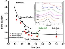 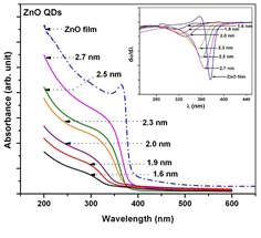
Room temperature optical absorption spectra of ZnO QDs of different sizes. Inset shows the first derivative of absorption spectra. Variation of exciton transition energy as a function of radius of ZnO QDs. The continuous curve shows the results of variation calculation including finite potential well width and exciton-phonon interaction. Inset shows typical TEM micrograph and SAED pattern of ZnO QDs.
3. ZnO nanorods
We have grown nearly vertically aligned ZnO nanowire array of mean diameter ~50-100 nm and length ~ 10s µm using high pressure PLD methodology. These vertically aligned nanowires of ZnO have promising applications in the area of sensors, lasers and vibration energy harvesting applications. SEM image of PLD grown ZnO nanowires is shown below.
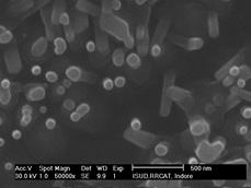
SEM image of vertically aligned ZnO nanowires
References:
- P. Misra et al., Alumina Capped ZnO Quantum Dots Multilayer Grown by Pulsed Laser Deposition, Solid State Commun. 127, 2003, 463-467.
- P. Misra et al., Room Temperature Photoluminescence from ZnO Quantum Wells Grown on (0001) Sapphire using Buffer Assisted Pulsed Laser Deposition, Appl. Phys. Lett. 89, 2006, 161912: 1 – 3.
- P. Misra et al., Temperature Dependent Photoluminescence from ZnO/MgZnO Multiple Quantum Wells Grown by Pulsed Laser Deposition, Superlattices and Microstructures, 42(1-6), 2007, 212-217.
- L. M. Kukreja et al., Nano - ZnO in Photonics Landscape, IEEE Proc. Photonics Global, ISBN: 978-1-4244-3901-0, 1 – 6 (2009)
- L. M. Kukreja et al., Anomalous optical processes in photoluminescence from ultra-small quantum dots of ZnO,J. Vac. Sci. Technol. A, 29(3), 2011, 03A120-8.
- P. Misra et al., Zinc Oxide Nanostructures: Growth, Characterizations and Applications; and L. M. Kukreja, Journal of Science, 8(1), 2011, 37-41.
- Amit K. Das et al., Effects of electron interference on temperature dependent transport properties of two dimensional electron gas at MgZnO/ZnO interfaces, Appl. Phys. Lett. 107 (10), 2015, 102104.
|


