| Accelerator Controls & Beam Diagnostics Division |
Timing (Delay Generator) Boards
|
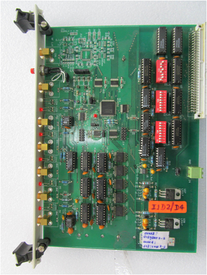
FPGA Based Course-Fine Delay Generator Board
- Five Channels Course-Fine programmable Delay generator board
- FPAG based VME (A24:D16) delay generator board with 5 channels.
- Delay of each channel is remotely adjustable in coarse and fine scale w.r.to input trigger.
- Board can be operated with external and on-board oscillator
- Fine delay resolution: 0.5 ns and Coarse delay resolution is governed by external clock/oscillator frequency
- Outputs are TTL with 50 Ohm line drive
- 5V VME DC voltage operated.
- Application: Indus-1 Timing control system
|
 |
| |
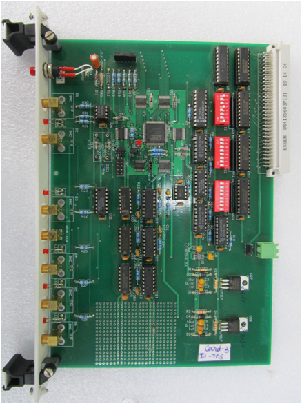
FPGA Based Course Delay Generator Board
- Five Channels Course delay Programmable Delay generator board
- FPAG based VME (A24:D16) delay generator board with 5 channels.
- Delay of each channel is remotely adjustable in coarse scale w.r.to input trigger.
- Board is with on-board oscillator
- Oscillator frequency governs the delay resolution
- Outputs are TTL with 50 Ohm line drive.
- 5V VME DC voltage operated
- Application:Indus-1 Timing control system
|
 |
| |
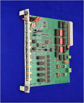
FPGA based Seven channel Course Fine delay generator board
- Seven Channels Course-Fine programmable Delay generator board.
- FPGA based VME (A24:D16) board.
- External and on-board clock.
- External trigger input is optically isolated
- Xilinx Spartan-3 FPGA is used to generate coarse delay and to realize other hardware logic
- Fine delay resolution: 0.5 ns and coarse delay resolution: 31 ns with booster RF clock at 31.613 MHz
- Outputs are TTL level with 50 Ohm line drive.
- Channel-to-channel jiter: < 200 ps.
- 5V VME DC voltage operated.
- Application:Indus-2 Timing control system.
|
 |
| |
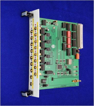
Coincidence and Revolution clock synchronized delay generator board
- FPGA based VME (A24:D16) delay generator board.
- This board generates coincidence clock (COIN) from of Indus-2 RF at 505.8 MHz and subsequent triggers synchronized to COIN Clock.
- It also generates REV CLK (1.73 MHz) from Indus-2 RF and produces multiple triggers SYN to REV CLK for Pinger Magnets in Indus-2 ring and other beam diagnostics devices.
- Mother board is configured for COIN trigger whereas daughter board for PM triggers.
- It has one I/P and 15 Output triggers
- Input trigger is optically isolated.
- ECL based high speed clock circuit handles input RF signal (505.8 MHz) to generate RF clock for COIN clock, further requirement of logic circuits in FPGA, on-board circuits etc..
- Delay is adjustable in coarse and fine scale
- Delay resolution 0.5 ns and channel-channel jitter < 150 ps
- 5V VME DC voltage operated.
- Application:Indus-2 Timing control system.
|
 |
| |
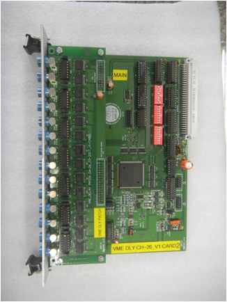
Multiple channels Trigger pulse generator board
- FPGA based VME (A24:D16) delay board.
- Multiple Trigger O/Ps: 26 Nos. Triggers are distributed in main and patch boards.
- REF Trigger I/P: External or internal. Frequency of REF trigger is programmable between 3- 9 kHz in internal mode.
- Provision for external PECL based clock circuit and on-board oscillator is kept. 125 MHz oscillator is used
- Trigger delay: Adjustable in coarse and fine scale
- Delay resolution: coarse 8 ns and fine 0.5 ns
- Trigger O/P:
- TTL level with 50 ohm line drive
- Pulse width is remotely settable: 2-9 µs
- Rise time: ~ 3 ns
- Channel-channel jitter ~ 200 ps
- 5V VME DC voltage operated.
- Application:BARC LPTD system
|
 |
| |
|
|


