|
Photo-Emission Electron Microscope Beamline on INDUS-2
Introduction:
Photo-Emission Electron Microscopy (PEEM) is a non-destructive imaging technique that involves shining linearly or circularly polarised X-rays onto the surface of a sample to provide spectroscopic information on nm scale. This information can be used to study nanostructures significant for sensors, catalysts, magnetic materials and nanoscale devices and phenomena such as nanomagnetism.
Laboratory-based imaging techniques such as STM, AFM and TEM are capable of resolving nanostructures but, (apart from a limited capacity with STM), are unable to provide spectroscopic information. PEEM can link a structure to its function by providing spectroscopic data on nm scale. The well-defined and variable polarisation state of synchrotron radiation can also provide, via dichroism, a contrast mechanism for imaging different magnetisations in ferromagnetic and antiferromagnetic nanostructures.
PEEM can be used to study the phenomenon of exchange bias, which has revolutionised the capabilities of magnetic information storage discs, where the underlying physical mechanisms are not well understood. There are also applications in the study of nano-particle catalysis, magnetic domain interactions and the characterisation of the properties of natural materials, such as chemical composition, local environment and phase identification. The fabrication and modification of novel materials on nm scale is another important area. Schematic of beamline is shown in Fig. 1.
Beamline layout:
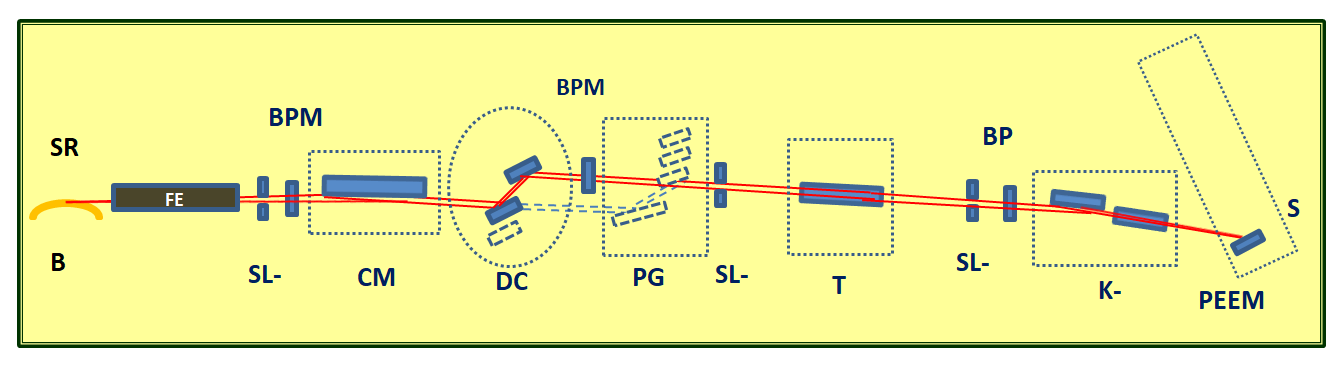
Fig. 1. A schematic layout of the PEEM beamline (top view) depicting various optical elements used; CM-Cylindrical Mirror, PG-Plane Grating monochromator, DC-double crystal monochromator , T-Toroidal mirror, K - K-B pair.
Beamline Specifications:
Source |
Bending magnet (2.5 GeV Indus-2 Source) |
Energy Range |
100 eV - 8 keV |
Monochromator |
Plane Grating Monochromator (M2 and GR) in low (100-2100 eV) energy range and Double Crystal Monochromator made of a pair of Si(111) crystals in (+, -) arrangement at higher energy range (2100 – 8000eV). |
Spot size @sample position |
HFWHM = 0.0273cm,VFWHM = 0.0064cm |
Photon flux [ph/s] |
~ 1011 ph/sec/0.1% bw |
Beam on the target |
Focussed |
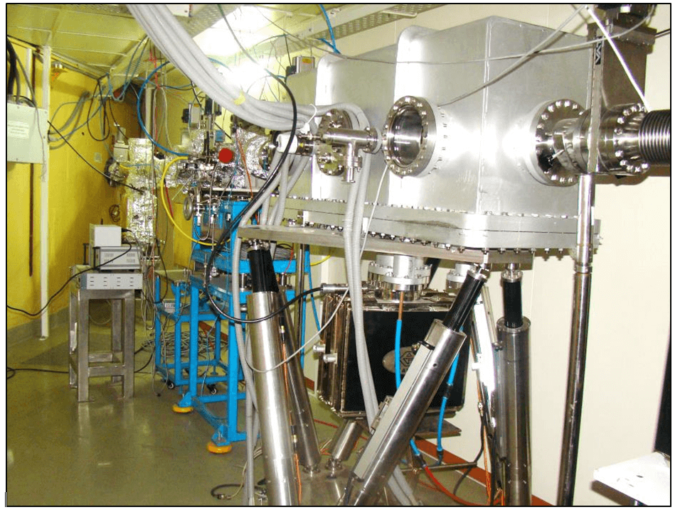
Fig. PEEM Beamline collimating mirror system.
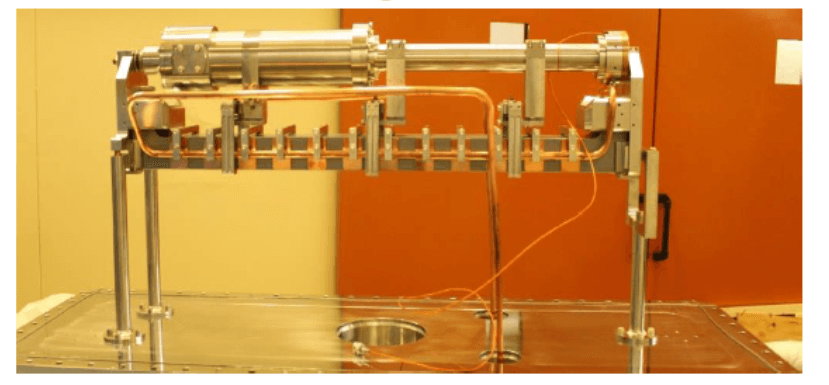
Fig. collimating mirror.
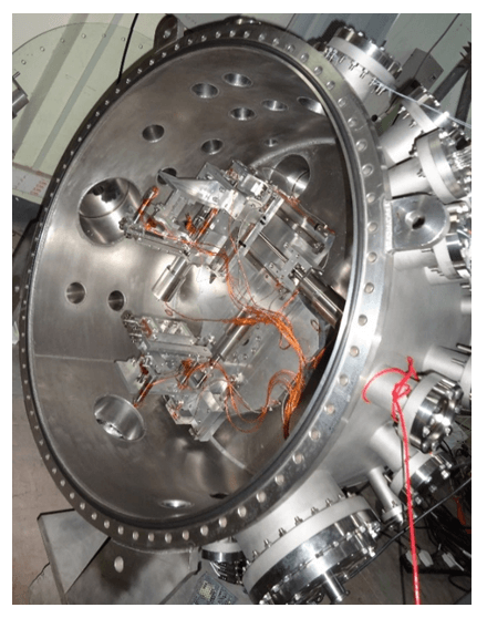
Fig. In-house developed Double crystal monochromator.
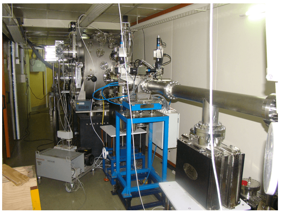
Fig. Double crystal monochromator and UHV line.
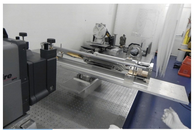
Fig. Toroidal mirror.
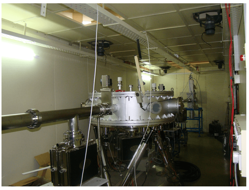
Fig. Toroidal mirror system.
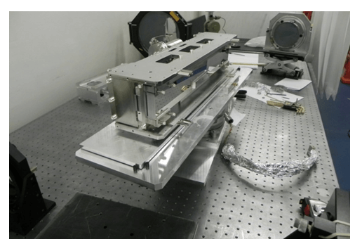
Fig. KB Mirror.
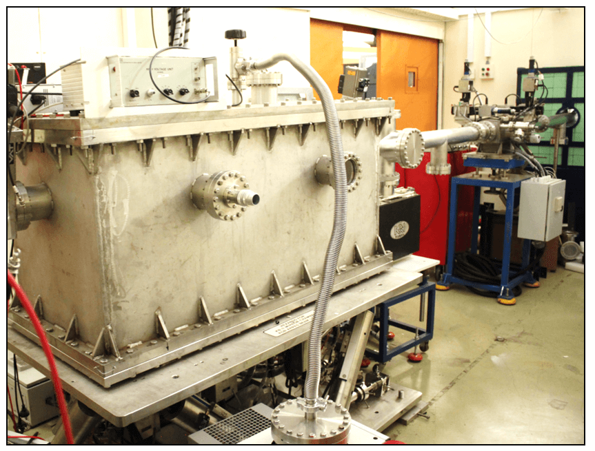
Fig. KB mirror system.
Experimental Station:
Experimental station of the PEEM consists of a photo-emission electron microscope
Microscope
The microscope will incorporate electron optic system consisting of mainly objective, intermediate, transfer and projection lenses with a high precision sample manipulator. These electrostatic lenses will be operating at very high voltages (typically~20 kV). Photograph of the PEEM lenses is shown below alongwith enlarged view of objective and projector lenses. The detector for PEEM beamline will be a slow scan CCD which can provide high spatial resolution images.
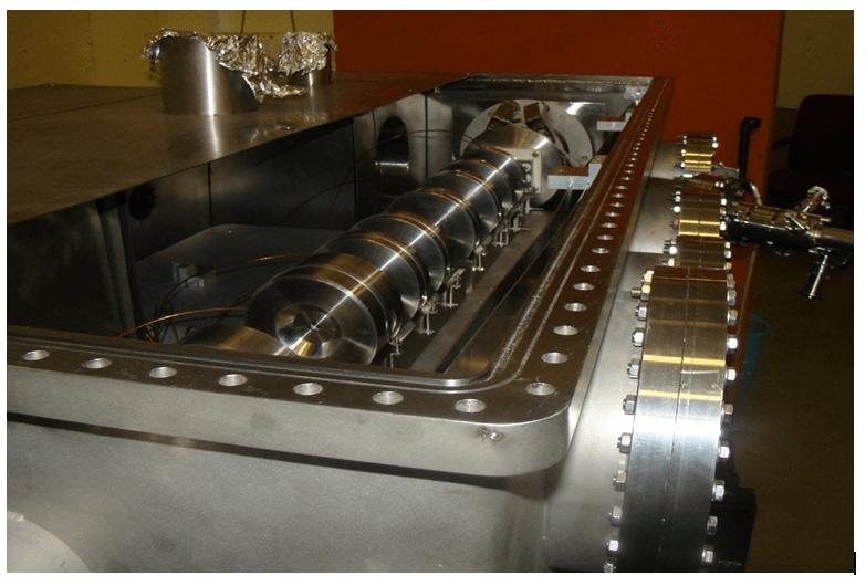
Fig. PEEM chamber with lenses .
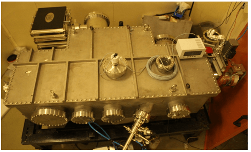
Fig. PEEM experimental station at the PEEM Beamline.
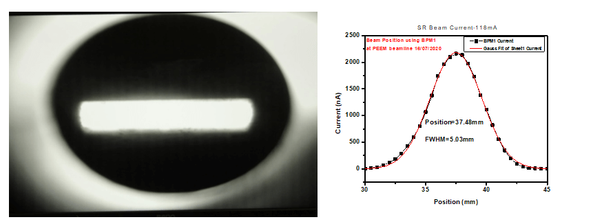
Fig. SR Beam first observed at BPM1 of PEEM Beamline.
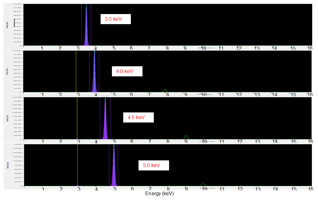
Fig. Monochromatic SR beam energy measured post DCM using Energy Dispersive Detector.
Present Status:
Presently, the alignment and testing of various key components of the beamline are underway
Contact Number : 91-731- 244 -2522/2118
In-charge: Shri U. K. Goutam ukgoutam@rrcat.gov.in
Other contributors:
Dr. Jagannath |
ssai(at)barc.gov.in |
Technical Physics Division
Bhabha Atomic Research Centre,
Mumbai – 400 085. |
Shri Kaushik Dutta |
kdutta(at)barc.gov.in |
Last Modification on: Sep 2020
| 


